LUCKY DRAGON TECHNOLOGY PCB&PCBA One-Stop Service
LUCKY DRAGON TECHNOLOGY PCB&PCBA One-Stop Service
The use of advanced processing equipment to meet the needs of customers in the high-end products, has a professional quality management team, the implementation of standardized, comprehensive quality management, and has a comprehensive testing equipment, process parameters and quality of the entire process of monitoring.
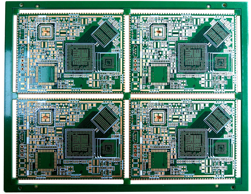
PCB board production types include: flexible circuit boards, rigid circuit boards, blind buried holes, etc., involving industrial control, automotive electronics, communications, smart home and other fields.
PCB Board Needs To Provide Information:
Gerber data, PCB board process requirements (sheet thickness, copper thickness, solder resist color, silk screen color, surface treatment process) and other special requirements;
PS:The impedance board needs to provide an impedance value.
Process Parameters
|
Project |
Sample |
Quantity |
|
Layers |
22-22 Layers |
4-12 Layers |
|
Min Width/Space |
3.0 mil / 3.0 mil |
4/4mil |
|
Board Thickness |
0.4-3.2mm |
0.6-3.2mm |
|
Min hole size |
Mechanical Hole:6.0 mil |
Laser Hole:8.0 mil |
|
Laser Hole:4.0 mil |
Laser Hole:4.0 mil |
|
|
Max Aspect Ratio |
10 : 1 |
8 : 1 |
|
Impedance control tolerance |
Single-ended 50ohm or less ±5ohm, differential below 72ohm ±15%, the remaining ±10% |
Single-ended 50ohm or less ±5ohm, differential below 72ohm ±15%, the remaining ±10% |
|
Outline Tolerance |
± 0.1 mm |
± 0.13 mm |
|
Materials |
FR-4, High TG, Halogen Free, Rogers, etc. |
|
|
Surface Finished |
HASL (Lead-Free), OSP, Electroplated Gold (Only Gold Finger ), Immersion Gold |
|
|
Special processing |
Rigid-flexible combination, mixed pressure, edge metallization, buried blind hole, back drill, half hole, impedance control, etc. |
|
|
Layers |
Normal Delivery(Sample) |
Expedited Delivery (Sample) |
Expedited VS Regular Spread |
|
Single/double panel |
3-4day |
24hours |
100% |
|
4 layers |
5-6day |
3-4day |
20-60% |
|
6 layers |
7-8day |
3-5day |
20-60% |
|
8 layers |
8-9day |
4-5day |
20-60% |
|
10 layers |
9-10day |
7-8day |
20-60% |
|
PS: 1. This delivery period does not include engineering processing time and order saturation status. Please contact our staff for the specific delivery period. |
|||


Products
|
|
4Layers PCB Materials: FR4 Tg170 Layers: 4 Hole Copper Thickness: 28um Copper Thickness: 1OZ Line width/Space: 4/4mil 3/3mil PCB Thickness: 1.2mm Minimun Hole size: 0.2mm Surface Finished: ENIG |
|
|
12 Layers PCB Materials: FR4 Tg170 Layers: 12 HDI Hole Copper Thickness: 22um Copper Thickness: 1OZ Line width/Space: 2.8/2.8mil 3/3mil PCB Thickness: 0.8mm Minimun Hole size: 0.1mm Surface Finished: ENIG+OSP PCB Size: 190mm*150mm |
|
|
6Layers PCB+FPCB Materials: FR4 + FPCB Layers: 6 Copper Thickness: 1OZ Line width/Space: 4/4mil 3/3mil PCB Thickness: 1.0mm Minimun Hole size: 0.3mm Surface Finished: ENIG |
|
|
2Layers Flexible Boards Materials: Flexible Boards Layers: 2 PI Thickness: 1.6mm Tolerance: ±0.03mm Surface Finished: ENIG PCB Size: 76mm*20mm |
Lucky Dragon Technology(SZ) Co.,LTD
4F, JinXin Building, No 326, LiuTang Road, Xin an Sub-District Bao an District, Shenzhen, Guangdong, China 518100
TEL: (86) 755 23074100
Email: Sales@Ldtac.com