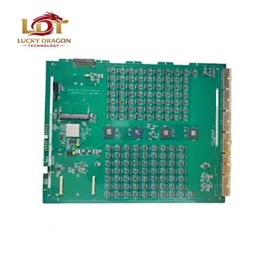
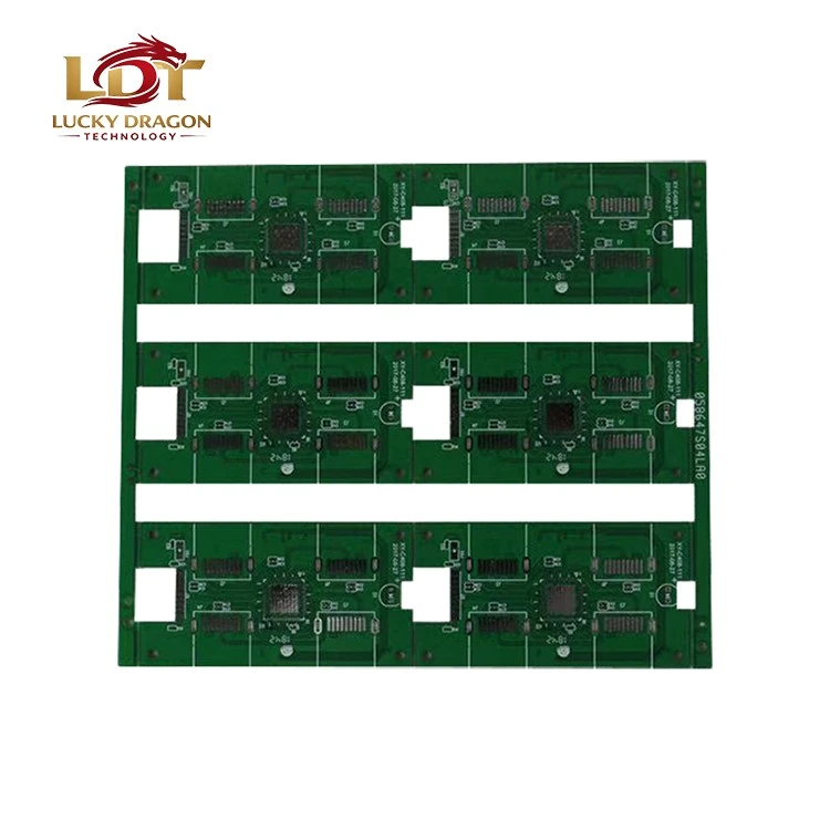
Engineered for low-loss signal propagation in high-frequency data transmission equipment, this high-speed communication PCB supports data rates from 25 Gbps to over 800 Gbps. Built utilizing ultra-low loss hydrocarbon ceramic thermoset and modified PTFE laminates, the architecture minimizes phase distortion, insertion loss, and dielectric dispersion across frequencies exceeding 10 GHz. Applied in core routing hardware, switch fabrics, and optical transport modules where signal integrity dictates system performance.
Technical Specifications
|
Parameter |
Specification Range |
|
Base Materials |
Rogers (RO3000, RO4000, RT/duroid), Panasonic (Megtron 6/7/8), Isola (I-Tera, Tachyon), Taconic |
|
Dielectric Constant (Dk) |
2.2 to 3.6 (at 10 GHz) |
|
Dissipation Factor (Df) |
0.0011 to 0.0040 (at 10 GHz) |
|
Layer Count |
2 to 44 Layers |
|
Finished Board Thickness |
0.5 mm to 6.0 mm |
|
Min. Trace Width / Spacing |
2.5 / 2.5 mil (0.064 mm) |
|
Min. Laser Drill Hole Size |
3.0 mil (0.075 mm) |
|
Impedance Control Tolerance |
±5% (Standard), ±8% (Tight Coupling) |
|
Surface Finish |
ENIG, ENEPIG, Immersion Silver, Immersion Tin, Hard Gold |
|
Max. Aspect Ratio |
Up to 18:1 |
Key Features
Controlled Glass Style Selection: Utilizes spread-glass and flat-glass weaves to eliminate local variations in dielectric constant caused by glass bundle unevenness.
Low-Roughness Copper Foils: Incorporates HVLP (High-Performance Very Low Profile) and RTF (Reverse Treated Foil) copper to minimize skin-effect conductor loss at high frequencies.
Precise Stack-Up Engineering: Matches dielectric thickness with copper weights to suppress electromagnetic radiation and inter-layer crosstalk.
Strict Registration Control: Employs optical alignment lamination presses to maintain layer-to-layer registration accuracy within ±10 um.
Applications
Data Center Core Switches and Enterprise Routers (100G / 400G / 800G ports)
5G NR Base Station Radio Units (RRU) and Active Antenna Units (AAU)
High-Density Optical Transceivers (QSFP-DD, OSFP architectures)
Satellite Communication (Satcom) Transceivers and Phased-Array Radar Front-Ends
Customization
Material Selection: Cross-referencing circuit simulation data against specific thermal and electrical parameters to select optimal hybrid stack-ups (e.g., combining high-speed laminates with standard FR-4 for cost-optimized multi-layer builds).
Backdrilling Depth Control: Stub removal via controlled-depth mechanical backdrilling to eliminate resonance points and reflections in high-speed via transitions.
Thermal Management Integration: Embedding copper coin technology, heavy copper planes, or thermal vias directly beneath high-dissipation transceiver ICs.
Quality Control
Impedance Testing
100% Time Domain Reflectometry (TDR) testing performed on test coupons accompanying every production panel.
Cross-Sectional Analysis
Microsection evaluation verifying copper plating thickness, barrel integrity, and dielectric void-free lamination.
Automated Optical Inspection (AOI)
High-resolution optical scanning of inner and outer layers for etch defects, shorts, and opens.
Flying Probe & Fixture Testing
Electrical continuity isolation testing executed on 100% of finished boards prior to shipment.
Manufacturing & Certifications
Production Infrastructure: Equipped with Orbotech direct imaging (LDI) systems, Schmoll high-speed mechanical drills, and Burkle vacuum lamination presses capable of multi-stage sequential lamination.
Process Cleanliness: Class 10,000 cleanroom environments dedicated to inner-layer dry-film transfer and lamination lay-up.
Certifications:
- ISO 9001:2015 (Quality Management System)
- IATF 16949:2016 (Automotive Quality Management)
- ISO 14001:2015 (Environmental Management)
- UL File Number: E354694 (V-0 Flammability Rating)
- IPC-A-600 Class 3 Acceptance Standard Compliance
Packaging & Delivery
Packaging Method: Vacuum-sealed anti-static shielding bags combined with moisture barrier bags (MBB) and silica gel desiccant packs. Individual boards separated by closed-cell EPE foam to prevent mechanical edge damage.
Traceability: Barcode labeling on individual packages containing production batch numbers, material lot IDs, and date codes.
Lead Times: Prototype builds (2–10 layers): 5–7 working days; Production runs: 12–20 working days depending on material availability.
FAQ
Q: How do you control batch-to-batch variations in dielectric constant (Dk) for Rogers or Megtron materials?
A: We source raw laminates exclusively from authorized primary distributors of Panasonic, Isola, and Rogers. Incoming material inspection verifies resin content, thickness tolerance, and supplier-provided test sheets. Stack-up designs are dynamically adjusted based on actual tested Dk values reported in the raw material batch certificate.
Q: What is your capability for microvia structures in high-layer count high-speed builds?
A: We execute up to 3+N+3 HDI stack-ups utilizing laser-drilled microvias down to 3 mil (0.075 mm). Sequential lamination cycles are controlled to maintain reliable via-fill plating performance and prevent inner-layer delamination during thermal stress tests.
Q: Can you process hybrid stack-ups combining ultra-low loss materials with standard FR-4?
A: Yes. Hybrid stack-ups integrate high-frequency laminates for signal layers and standard FR-4 (such as high-Tg FR-4) for power and ground planes to reduce overall material costs. Coefficient of Thermal Expansion (CTE) matching is evaluated during pre-production engineering to prevent board warp during assembly reflow.
Q: How is controlled-depth backdrilling tolerance maintained?
A: Backdrilling is performed using specialized mechanical drilling systems with optical depth-sensing mechanisms. Stub lengths are controlled to within ±0.15 mm (6 mil) from the target inner-layer copper plane, effectively suppressing signal reflections at frequencies above 10 GHz.
Q: What is your standard impedance tolerance and test verification process?
A: Our standard controlled impedance tolerance is ±5% for critical single-ended and differential traces (50 ohms / 100 ohms). Every production panel includes dedicated test coupons tested via TDR equipment. TDR impedance reports are archived and supplied alongside the shipment documentation.
Q: What file formats are required to initiate a DFM review for an RF/High-Speed PCB?
A: Gerber RS-274X or ODB++ fabrication data must be accompanied by an explicit stack-up drawing detailing copper weights, dielectric material part numbers, target impedance values with allowable tolerances, and specific surface finish requirements.
Request a Quote
Submit your Gerber/ODB++ files, stack-up requirements, and material preferences for a DFM evaluation and quotation within 24 hours.
[Upload Gerber Files & Request Quote]
Hot Tags: high-speed communication pcb, China high-speed communication pcb manufacturers, suppliers, factory