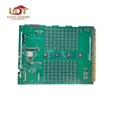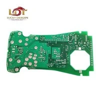

High-speed server PCBs provide the high-frequency interconnect backbone for enterprise computing and data center infrastructure. Built for PCIe Gen 5/6 and 112G PAM4 signaling environments, these multilayer boards minimize signal degradation, dielectric loss, and electromagnetic interference (EMI) across dense server architectures.
Technical Specifications
|
Parameter |
Specification Range |
|
Layer Count |
4 to 40 layers |
|
Board Thickness |
1.0mm to 6.0mm (Aspect ratio up to 20:1) |
|
Material Types |
Low-Dk/Df laminates (Panasonic Megtron 6/7/8, Isola Astra MT77, Rogers RO4000 series) |
|
Impedance Tolerance |
+/-5% (Single-ended & Differential) |
|
Minimum Trace / Space |
3 mil / 3 mil (0.075mm) |
|
Copper Weight |
0.5 oz to 3 oz (HVLP and VLP copper foil available) |
|
Surface Finish |
ENIG, Immersion Silver, OSP, ENEPIG |
|
Via Technology |
Laser microvias, stacked/staggered blind and buried vias, controlled depth back-drilling (stub length < 0.2mm) |
Key Features
Ultra-Low Dielectric Loss: Utilizes low-Dk (< 3.8) and low-Df (< 0.005) resin systems to suppress signal attenuation at frequencies exceeding 28 GHz.
Controlled Copper Roughness: Employs Very Low Profile (VLP) and Hyper Very Low Profile (HVLP) copper foils to mitigate skin effect losses and insertion loss at high data rates.
Precision Back-Drilling: Eliminates parasitic stub capacitance on through-hole vias, preserving signal integrity for high-speed serial links.
Glass Weave Skew Mitigation: Incorporates spread glass styles and mechanical rotation stack-ups to prevent differential pair propagation delay variations.
Applications
AI/ML Server Motherboards (NVIDIA/AMD accelerator boards)
Enterprise Blade Servers and Rackmount Servers
400G / 800G Data Center Core Switches and Routers
High-Performance Storage Area Network (SAN) Controllers
Customization
Stack-Up Optimization: Engineering support for impedance modeling and dielectric spacing adjustments based on customer simulation data (HyperLynx, ADS).
Material Selection: Cross-referencing thermal and electrical requirements to select matching prepreg and core combinations.
Specialized Constructions: Hybrid stack-ups combining high-speed laminates with standard FR-4 for cost-optimized routing layers.
Quality Control
Impedance Testing: TDR (Time Domain Reflectometry) testing performed on every production panel using dedicated test coupons.
Signal Integrity Validation: Vector Network Analyzer (VNA) testing available for insertion loss and return loss verification up to 50 GHz.
Internal Inspection: Automated Optical Inspection (AOI) for inner layers, X-ray inspection for layer-to-layer registration, and destructive microsection analysis for plating thickness verification.
Reliability Testing: Thermal shock testing, solder float testing, and peel strength measurements executed per IPC-TM-650 protocols.
Manufacturing & Certifications
Facility Equipment
Direct Imaging (DI) exposure systems, high-precision CNC routing machines, laser drilling systems, and vacuum lamination presses.
Process Control
Cleanroom environment for inner layer dry film imaging and lamination lay-up to eliminate particulate defects.
Certifications
ISO 9001, ISO 14001, IATF 16949, UL-listed (E-number tracking), and RoHS/REACH compliant manufacturing processes.
Packaging & Delivery
Packaging: Vacuum-sealed anti-static ESD bags with desiccant packs, cushioned with EPE foam inside double-walled corrugated export cartons.
Traceability: Barcode labeling on each master carton indicating part number, revision, date code, and batch quantity.
Lead Time: Prototypes delivered in 5 to 8 business days; volume production scheduled via Kanban or forecast-based release programs.
FAQ
Q: How do you control glass weave skew in high-speed server PCBs?
A: We utilize mechanically spread glass styles (such as 1078 or 2116 with low-profile weaves) and implement diagonal routing or staggered glass warp/fill orientations during the CAM layout phase to equalize the dielectric constant across differential pairs.
Q: What is your standard capability for back-drilling stub control?
A: Our controlled-depth back-drilling process maintains a residual stub length of less than 0.2mm (8 mils), effectively eliminating stub resonance in 56G and 112G serial channels.
Q: Can you process hybrid stack-ups combining Rogers and standard FR-4 materials?
A: Yes. We routinely process hybrid constructions (e.g., Rogers high-frequency outer layers with Megtron or FR-4 inner layers) utilizing specialized surface preparation and bonding parameters to ensure reliable inter-laminate peel strength.
Q: What data formats do you require for impedance-controlled builds?
A: We require Gerber RS-274X or ODB++ fabrication data, along with a detailed stack-up drawing specifying target impedances, reference planes, and specific material part numbers or target Dk values at designated frequencies.
Q: How do you verify inner layer alignment on high layer-count boards (24+ layers)?
A: We utilize X-ray alignment systems during the lamination lay-up process and apply scaled artwork compensation based on material movement data gathered from pre-production laser registration tests.
Q: What is the typical lead time for NPI batches versus mass production?
A: New Product Introduction (NPI) prototypes typically require 5 to 8 days depending on layer count and material availability. Volume production batches are scheduled on a 2-to-4-week standard production cycle, with vendor-managed inventory (VMI) options available for recurring demand.
Request a Quote
Upload your Gerber files, stack-up requirements, and material specifications below to receive a DFM review and formal quotation within 24 hours.
[Upload Gerber Files & Request Quote]
Hot Tags: high-speed server pcb, China high-speed server pcb manufacturers, suppliers, factory