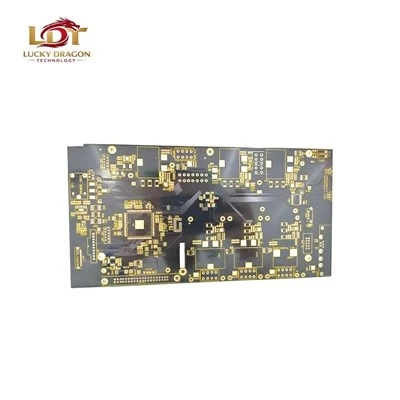
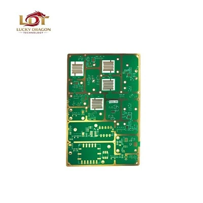
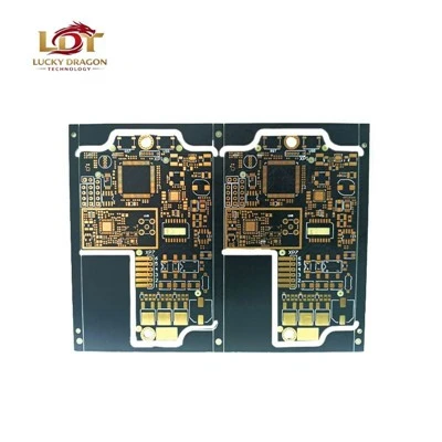
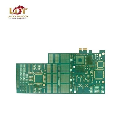
Build-to-Spec Custom Rigid PCBs | IPC-6012 Class 3 / Class 3/A Compliant
Structure Types: 1+n+1, 2+n+2, 3+n+3, Any-layer (ELIC - Every Layer Interconnect).
Layer Count: 4 to 24 layers (HDI core build-ups).
Core Material Dk/Df Alignment: FR-4 (Tg >= 170°C), Low-loss hydrocarbons (Rogers RO4000 series), High-speed low-Df laminates (Panasonic Megtron 4/6/7, Isola Tachyon 100G).
Primary Value Delivery: High I/O density BGA pitch breakout (<= 0.4 mm pitch), controlled impedance integrity up to 28/56/112 Gbps PAM4, reduced layer count vs. standard multi-layer via blind/buried schemes.
|
Parameter |
Capability / Range |
Production Limit / Tolerance |
|
Max Layer Count |
24 layers |
Stackup-dependent |
|
Min Line Width / Space (L/S) |
Inner: 2/2 mil (50 µm), Outer: 3/3 mil |
Etching tolerance ± 0.5 mil |
|
Laser Via Diameter |
3 mil to 6 mil (75–150 µm) |
Aspect ratio <= 0.8:1 |
|
Stacked / Staggered Vias |
Up to 3-level stacked via-in-pad |
Filled with conductive/non-conductive epoxy & capped |
|
Finished Board Thickness |
0.4 mm to 3.2 mm |
± 10% overall thickness |
|
Controlled Impedance |
50 Ω single-ended, 100 Ω diff pair |
± 10% standard (± 5% tight control on request) |
|
Surface Finish |
ENIG, ENEPIG, Immersion Ag, Immersion Sn, OSP, HASL (lead-free) |
IPC-PL-09 / IPC-4552 specs |
|
Max Panel Size |
530 mm × 610 mm |
Effective routing area per panel rule |
Sequential Laser Ablation
UV/CO2 hybrid laser routing enables targeted microvia formation without thermal stress cracking on adjacent dielectrics.
Via-in-Pad Copper Plating
Planarized via filling (via filling depth depression < 15 µm) prevents solder wicking and ball-grid-array (BGA) voiding during reflow.
Controlled Resin Flow Prepreg
Ultra-thin prepregs (2 mil to 3 mil) paired with laser-drilled sub-composites suppress internal void nucleation in high-layer-count builds.
Laser Direct Imaging (LDI)
Registration tolerance ± 15 µm layer-to-layer alignment for tight pitch BGA packages.
|
Sector |
Specific Application |
Critical Technical Driver |
|
Telecom / Datacom |
5G RU baseband boards, 100G/400G optical modules |
Low insertion loss (Df <= 0.004), skew control |
|
AI / High-Speed Computing |
GPU/ASIC accelerator carrier boards |
High-density power/ground plane partitioning, 0.4 mm pitch BGA |
|
Medical Electronics |
Ultrasound probe beamformers, portable defibrillators |
High reliability Class 3/A, micro-miniaturization |
|
Industrial / Robotics |
Servo drive controllers, multi-axis motion feedback |
High vibration resilience, thermal dissipation via thermal vias |

Stackup Co-Design: Submit schematic, stackup target, or netlist; engineering returns finalized stackup with Df/Dk compensation and impedance profile within 24 hours.
Plug Material Options: Copper-filled conductive paste (via filling resistivity < 25 µΩ·cm) vs. non-conductive epoxy (Epoxy Technolog/San-Ei).
Selective Plating: Selective gold thickness up to 30 µin on edge connectors while maintaining standard ENIG on BGA pads.
Routing Modification: DFM exception waivers processed with direct engineering sign-off.
AOI (Automated Optical Inspection): 100% inner/outer layer line width/space verification post-etch.
XRF (X-ray Fluorescence): Thickness verification per lot (ENIG Au 2–4 µin, Ni 120–240 µin).
Microsection Analysis: 3 samples per production batch verified for copper barrel thickness (> 20 µm min), resin fill height, and thermal stress integrity (288°C, 10 seconds, 3 cycles per IPC-TM-650 2.6.8).
Electrical Test: 100% flying probe test (for prototype <= 50 pcs or high-density low volume) or fixture-based bed-of-nails (for volume > 1000 pcs). Isolation threshold > 10 MΩ at 250V/500V.
Dongguan manufacturing facility | 18,000 m² cleanroom environment | Monthly capacity: 45,000 m² multi-layer/HDI panels. Class 10,000 cleanroom exposure areas for inner-layer dry film lamination and laser drilling.
Orbotech Paragon LDI systems
Hitachi UV/CO2 dual-head laser drill stations
Atotech direct vertical continuous plating (VCP) lines
ISO 9001:2015
IATF 16949:2016 (Automotive electronics subset lines)
ISO 13485:2016 (Medical device quality compliance)
IPC-6012 Class 3 (default for high-reliability/HDI), IPC-A-600 Class 3 acceptance criteria.
RoHS directive compliant, REACH SVHC declaration ready, CMRT conflict minerals reporting supported.
Vacuum Sealing
Anti-static moisture-barrier bags (MBB, < 0.02 g/m²/24h WVTR) with Indicating Humidity Indicator Cards (HIC) and Type A molecular sieve desiccant.
Physical Protection
Edge-buffered corrugated cartons with individual closed-cell foam interleaving; warp-preventing clamping fixtures for thin boards (< 0.8 mm).
Lead Times
Prototype (1–3n+1): 5–7 working days (standard review) / 3 working days (expedited NPI).
Volume Pilot Run: 10–14 working days post-PPAP sign-off.
Logistics
DDP / EXW / FOB via DHL/FedEx Express (air freight prototype) or palletized ocean freight (volume).

Commercial & Volume Tiers:
Prototype / NPI: 5–25 pcs (3–5 working day turn)
Pilot Run: 50–500 pcs (MOQ flexible per stackup complexity)
Volume: 1,000+ pcs (consignment or bonded stock scheduling available)
With abundant experience, we are one of the most professional hdi pcbs manufacturers and suppliers in China. We warmly welcome you to buy bulk high quality hdi pcbs for sale here from our factory. If you have any enquiry about cooperation, please feel free to email us.