Lucky Dragon Technology Shenzhen Co., Ltd.
+86-755-23074100
Contact Us
  • TEL:+8618948705000
  • Email:sales@Ldtac.com
  • Add: 5th Floor, Building 1, Jinshan Industrial Park, 375, Xixiang Section, Guangshen Road, Xixiang Street, Baoan District, Shenzhen City, Guangdong Province, China

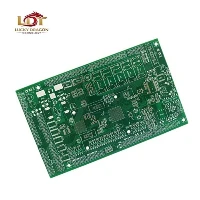
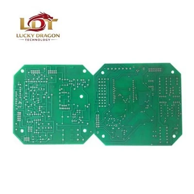
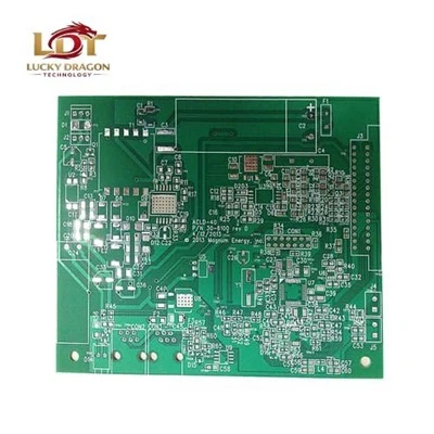
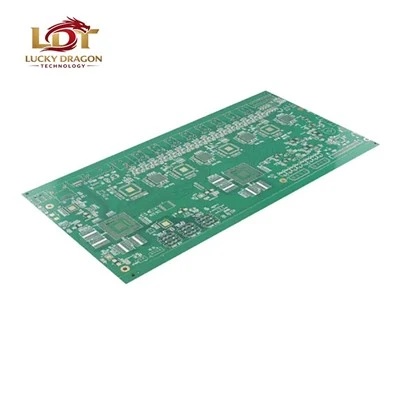
Multilayer PCBs (4–32 Layers) | Rigid Custom Printed Circuit Boards


Precision-engineered multilayer stackups for industrial, medical, and high-reliability OEM hardware. Built to IPC-A-600 Class 2/3. Impedance-controlled down to +/-10%. ITAR-exempt commercial supply chain.


Product Overview

Parameter

Specification Profile

Layer Count

4 to 32 layers (even stackups standard; odd stackups on review)

Board Types

Standard rigid, HDI (Any-layer / 1+N+1), High-frequency (Rogers/Taconic hybrid)

Standard Volume Lead Time

Prototype: 5–7 days

Data Intake

Gerber RS-274X, ODB++, IPC-2581; NC Drill (Excellon), IPC-D-356 netlist


Technical Specifications

Feature Category

Production Capability / Limit

Standard Tolerance / IPC Class

Finished Thickness

0.4mm - 4.5mm

+/-10% (overall)

Min Trace / Space

3.0 mil / 3.0 mil (0.075mm / 0.075mm)

+/-20% or +/-0.5 mil

Min Laser Via (HDI)

0.1mm (4 mil) blind/buried

IPC-6012 Class 2/3

Min Mechanical Hole

0.15mm (6 mil)

+/-0.05mm plated

Copper Weight (Inner/Outer)

0.5 oz to 4 oz finished

IPC-2221 compliance

Surface Finishes

ENIG (IPC-4552), OSP (IPC-4553), Immersion Ag, Hard Gold (edge connectors)

Thickness certified via XRF

Solder Mask

LPI (Green, Black Matte, Blue, Red, White)

IPC-SM-840E

Impedance Control

Single-ended (50 ohm), Differential (90 ohm / 100 ohm)

+/-10% TDR verified coupon

Base Laminate Materials

Isola (FR408HR, 370HR), Ventec (VT-47), Panasonic (MEGTRON 6), Rogers (RO4350B)

Tg >= 170 degC for high layer count


Key Features
 

Controlled Dielectric Stackup

Symmetric prepreg/core sequencing matched to TDR simulation reports prior to lamination press.

Via-in-Pad Electroplating

Resin-filled and copper-plated over via process for high-density BGA breakout (0.4mm pitch).

High-Tg Thermal Resilience

Thermal stress survival through 6x lead-free IR reflow profiles (260 degC peak) without delamination or barrel cracking.

Edge Plating / Castellated Holes

Plated half-holes (0.6mm min diameter) for daughter-to-motherboard vertical plug-in modules.


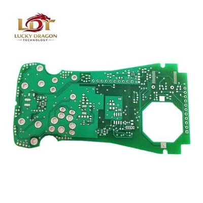
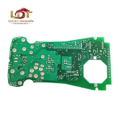
Multilayer PCBs


Applications

Industrial Automation: PLC backplanes, multi-axis motion controller boards (6–12 layers, heavy 2 oz power planes).


Telecommunications: Core switch linecards, high-frequency RF transceiver modules (hybrid FR4/Rogers 16–24 layers).


Medical Diagnostic Hardware: Ultrasound frontend signal processing, patient monitor data acquisition motherboards (low-noise ground stitching).


Automotive Subsystems: LiDAR interface boards, battery management system (BMS) supervisory PCBs (IPC-A-600 Class 3).


Customization & Engineering Support


1

DFM/DFAsing Review Scope

24-hour turnaround engineering query report highlighting annular ring violations, acid traps, unanchored copper, and aspect ratio risks (>10:1 drill depth-to-diameter requires secondary evaluation).

2

Stackup Customization

Supply target impedance values (Z0) and stack height constraints; engineering generates impedance coupon design per layer.

3

Panelization

Customer-defined fiducials, tool holes (3.175mm), V-cut depth/web tolerances (0.3mm +/-0.05mm), or tab-routing with break-away mousebites.

4

Buffer Stock & VMI Management

Dedicated safety stock programs (customer-owned or fab-held bonded inventory) for long-lead specialized materials (Rogers / Megtron 6) to eliminate volume run line-stops.


Quality Control


Inspection & Test Gateways

AOI (Automated Optical Inspection): Inner layers post-etch, outer layers post-solder mask.
Flying Probe Test: Nets verified on 100% of prototypes (< net resistance thresholds).
E-Test (Fixture): Applied for batch runs >250 pcs.
Microsection Analysis: Destructive physical analysis per lot for plating thickness, barrel copper uniformity (>20 um min barrel wall for Class 3), and dielectric spacing.

Traceability

Laser-etched date code, batch tracking, and material COC (Certificate of Conformance) stored digitally per lot.

Multilayer PCBs


Manufacturing & Certifications

Plant Profile & Footprint:

  • Facility Location: Export-compliant commercial manufacturing base (ITAR-exempt commercial supply chain, Asia/Global export logistics hub).
  • Lamination press lines: 4 high-temp vacuum hydraulic presses.
  • Laser drilling: Schmoll/Orbotech UV/CO2 laser drill rigs.
  • Plating line: Vertical continuous plating line with periodic pulse reverse (PPR) copper distribution.


Compliance Standards: ISO 9001:2015, IATF 16949 (secondary automotive scope), ISO 13485 (medical subset), UL E-file certified, RoHS/REACH compliant.


Packaging & Delivery


Packaging Standard: Vacuum-sealed anti-static ESD bags (<10^11 ohm/sq), silica gel desiccant packs, humidity indicator card (HIC), double-walled corrugated cartons with 50mm corner foam inserts. Baking protocol applied (120 degC for 4–24 hours) prior to vacuum seal if shelf-life window requires.


Logistics: FOB / EXW / DDP via DHL/FedEx Express (prototypes) or palletized air/sea freight (volume batch). Commercial invoice, packing list, COC, and microsection report included in shipment documentation.


FAQ


Q: What is your maximum aspect ratio for through-hole plating on 16+ layer boards?

A: Standard aspect ratio limit is 10:1 for mechanical drilling (0.2mm drill via 2.0mm board thickness). For higher aspect ratios up to 14:1, processing requires specialized entry material and sequential descering review.

Q: Do you charge extra for impedance coupon fabrication and TDR test report?

A: Impedance coupon integration on manufacturing panel waste space is included at no extra charge for orders requiring controlled impedance specs; TDR test report summary is checked and attached to the shipping dossier.

Q: How do you handle mixed dielectric stackups (e.g., Rogers high-frequency core with FR4 prepreg)?

A: Material stackup requires thermal expansion coefficient (CTE) balancing. We substitute matching high-Tg prepreg bondplies (e.g., FR408HR resin system) to prevent delamination during z-axis thermal stress. Submit stackup proposal or let our PE team propose pre-lamination balance.

Q: What file format discrepancy halts line processing?

A: Missing drill list, unassigned NC tool rack units, or Gerber coordinate mismatch (inch vs. metric scale offset). Our DFM hold notice pauses production within 4 hours of data intake.

Q: Can you support VMI/buffer stock programs for long-lead Rogers/Panasonic laminates during volume ramps?

A: Yes. For annual forecasts involving constrained dielectrics (>6 weeks raw material lead time), we establish fab-held safety stock rolling agreements tied to your forecasted release schedule.


modular-1
Request a Quote

Direct PE technical response within 4 working hours (auto-routed across GMT, CET, and EST coverage desks via
Required Input Checklist:
Gerber files (RS-274X) + Excellon drill file
Stackup requirement or target finished thickness (mm)
Surface finish selection (ENIG, OSP, etc.)
IPC Class requirement (Class 2 or Class 3)
Target volume (Prototype / Pilot / Annual forecast with VMI preference) and required delivery date

With abundant experience, we are one of the most professional multilayer pcbs manufacturers and suppliers in China. We warmly welcome you to buy bulk high quality multilayer pcbs for sale here from our factory. If you have any enquiry about cooperation, please feel free to email us.

(0/10)

clearall