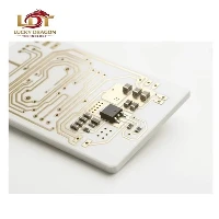
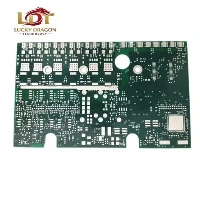
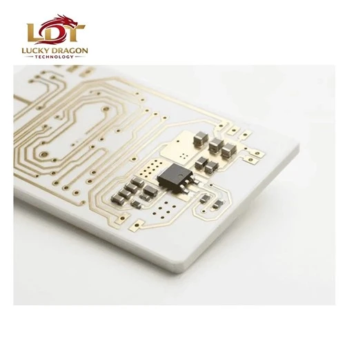
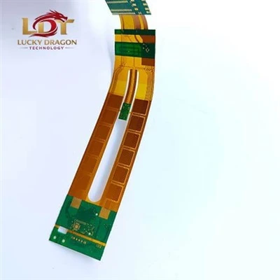
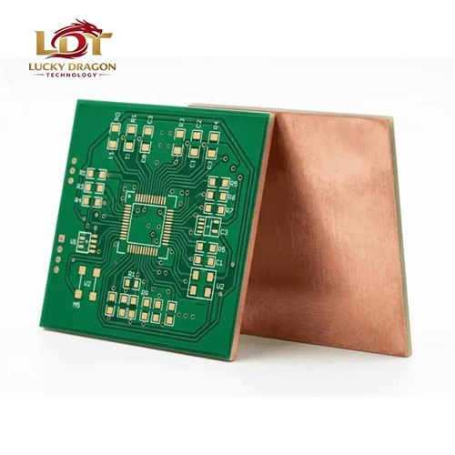
High-Current Power Distribution & Thermal Integration Printed Circuit Boards
Heavy copper PCBs incorporate copper weights from 3 oz (105 um) to 20+ oz (700 um) per layer, laminated within multi-layer or single/double-sided architectures. Engineered for continuous high-current power routing (50A-400A+) and direct thermal extraction from high-power MOSFETs/IGBTs/SIC modules without external busbars.
Core Capability Envelope: 1 to 12 layers (heavy power planes mixed with fine-pitch signal/control layers); outer layer heavy copper up to 15 oz, inner layer up to 20 oz.
Primary Differentiator: Proprietary differential wet-etch compensation and multi-stage step-plating profiles suppressing copper thickness gradient variation across large-format industrial panels (500 x 600 mm).
|
Parameter |
Capability / Range |
Production Note / Limit |
|
Copper Weight (Finished) |
Outer: 3 oz - 15 oz Inner: 3 oz - 20 oz |
Mixed stackups (e.g., 10 oz power + 1 oz control) supported |
|
Min. Track / Gap (>= 4 oz) |
Track: 6 mil - 10 mil Gap: 8 mil - 12 mil |
Scales with finished copper weight; etching factor controlled |
|
Max Board Dimension |
500 mm x 600 mm |
Panel utilization affects panel-edge copper thinning |
|
Layer Count |
1 to 12 layers |
Inner-layer heavy copper requires heavy resin-content prepreg (7628 / 2113 mix) |
|
Substrate Materials |
High-Tg FR-4 (Tg >= 170 deg C), CEM-3, Ceramic-filled hydrocarbon (Rogers RO4003C / TC series) |
Mandatory peel-strength verification >= 1.2 N/mm |
|
Surface Finish |
ENIG, ENEPIG, Immersion Silver, OSP, HASL (Lead-free) |
ENIG preferred for heavy-copper wire-bonding / power-module contact pads |
|
Thermal Vias / Inlays |
Solid copper filled/capped plugged vias, press-fit holes |
Void-free X-ray acceptance criteria per IPC-A-600 Class 3 |
Zero-Busbar Hybrid Integration
Consolidates copper busbars directly into FR4/ceramic stackups, reducing mechanical fastener count by 60% and eliminating vibration-loosened screw terminals.
Controlled Etching Sidewall Profile
Trapezoidal angle <= 15 deg maintained on >= 6 oz tracks, preventing solder mask bridging during mass-reflow of QFN/TO-247 packages.
Thermal-Gradient Mitigation
High-resin-flow prepreg sequence fills deep interstitial voids between thick copper planes, eliminating micro-voids prone to moisture absorption or high-voltage tracking.
High-Current Thermal Spreading
Thermal resistance (R_thetaJC) reduction of 35% compared to standard 1-oz boards with thermal via arrays.

EV/HEV Power Inverters: DC-link capacitor interface and 3-phase bridge gate-driver/power-stage integration.
Industrial Motor Drives (VFDs): 480V-690V high-current output stages carrying 150A continuous phase current.
Renewable Energy Infrastructure: Solar string inverter DC combining nodes and wind-turbine pitch-control motor driver boards.
High-Power Welding & Plasma Cutters: High-frequency switching transformer windings and high-current rectifier bridges.
Stackup Engineering Review: Submit Gerbers + expected continuous/surge current profiles (I_rms, I_peak) for copper-weight optimization.
DFM Violation Redlining: If DFM audit flags copper/space violation on >= 6 oz, our AE team provides a redlined Gerber feedback with 3 stackup alternatives within 16 hours.
Local Copper Thickening (Selective Plating / Step Plating): Heavy copper restricted to high-current zones; standard 1 oz-2 oz retained in fine-pitch IC breakout regions.
Cavity & Depth Milling: Controlled-depth milling for direct semiconductor die-attach or busbar terminal pockets.
Prototypes Modification Turnaround: Prototype build 10-12 business days post-DFM sign-off.
Quality Control & Inspection Standards
Material Traceability
Material Certificate of Conformance (CoC) + Laminate Lot Manufacturer Batch ID supplied standard with shipment, supporting full IPC-1791 / supply-chain traceability on request.
IPC Compliance
Manufactured per IPC-6012 Class 3 / Class 3/A (High Reliability / Automotive space).
Process Inspection Gate
X-Ray Fluorescence (XRF): Nickel/Gold or Surface finish thickness verification per batch.
AOI + Automated Laser Profilometry: Copper thickness and surface planarity map post-etch.
Microsection Analysis (Destructive): Plated-through-hole copper barrel wall thickness (>= 25 um min local), thermal shock test (288 deg C solder float 10 seconds x 3 cycles) per IPC-TM-650 2.6.8.
High-Potential (Hi-Pot) Dielectric Withstand: Tested per design voltage profile (e.g., 2.5 kVAC / 60s for isolation gaps).
Manufacturing & Facility Baseline
Etching Line
Horizontal high-pressure conveyor spray etch with real-time cupric chloride / ferric chloride regeneration and density/temperature closed-loop feedback.
Plating
Direct DC/Pulse reverse periodic plating lines with dedicated high-aspect-ratio pulse rectification for uniform barrel distribution in heavy-copper PTH.
Certifications
ISO 9001:2015, IATF 16949:2016 (Automotive quality management system), ISO 13485 (optional/medical power), UL-listed (E-file tracking active).
Humidity Control
Vacuum-sealed anti-static ESD bags with 30%-40% RH silica gel desiccant and humidity indicator card (HIC).
Physical Protection
Interleaved EPE foam sheets; edge-board cardboard corner protectors; custom heavy-duty export carton or fumigated wooden pallet.
Traceability Labeling
Barcoded roll/box labels listing Date Code, Batch/Lot ID, Copper Weight Class, and UL Logo.
Shipping Terms
FOB Shenzhen / CIF European & North American main ports via air freight (DHL/FedEx express for prototypes, DHL/UPS or air charter for volume) or sea freight container.

To lock in a DFM review and quotation within 24 working hours, provide:
Gerber / ODB++ Package + Drill file + Stackup layer specification.
Copper Weight Target: Outer/Inner oz per layer.
Volume Profile: Prototype quantity + Estimated annual volume (EAV) or blanket release schedule.
Compliance / Standard Requirement: IPC Class 3, IATF 16949 PPAP Level 3 documentation requirement (Yes/No) / FAI package scope.
Target Delivery Port / Destination Zip Code.
With abundant experience, we are one of the most professional heavy copper pcbs manufacturers and suppliers in China. We warmly welcome you to buy bulk high quality heavy copper pcbs for sale here from our factory. If you have any enquiry about cooperation, please feel free to email us.