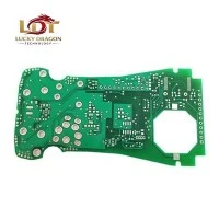
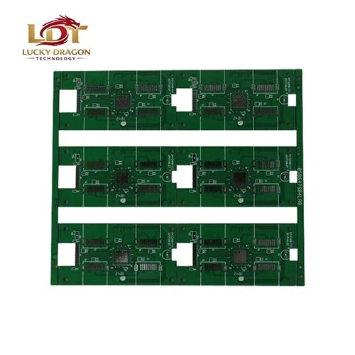
High-speed PCBs are precision-engineered multi-layer printed circuit boards built for high-frequency signal integrity and low-loss transmission. Designed to support multi-gigabit data rates (25Gbps to 112Gbps+ NRZ/PAM4), these boards utilize specialized low-Dk/Df laminate materials, tightly controlled copper roughness, and advanced impedance matching. Manufactured in an ISO 9001 and IATF 16949 certified facility, production lines feature laser direct imaging (LDI), controlled impedance testing via TDR, and automated optical inspection (AOI) to meet strict IPC Class 3 standards for data center, telecom, and automotive infrastructure. Scaling from single-piece rapid prototypes to volume production runs exceeding 100,000 units, manufacturing workflows accommodate both agile engineering validation and stable commercial supply.
|
Parameter |
Specification Range |
|
Max Layer Count |
Up to 40 Layers |
|
Dielectric Constant (Dk) |
2.2 to 3.8 (at 10 GHz) |
|
Dissipation Factor (Df) |
0.0011 to 0.0050 |
|
Impedance Tolerance |
+/- 5 percent (Tight control down to +/- 3 percent available) |
|
Min Trace/Space |
3.0 mil / 3.0 mil (75 um / 75 um) |
|
Min Laser Via Size |
3.0 mil (75 um), Stacked/Staggered Microvias |
|
Board Thickness |
0.20 mm to 6.0 mm |
|
Max Panel Size |
600 x 700 mm |
|
Copper Foil Types |
RTF (Reverse Treated Foil), VLP, HVLP, ED Copper |
|
Surface Finishes |
ENIG, ENEPIG, Immersion Silver, Immersion Tin, OSP |
Controlled Dielectric Constants
Utilizes hydrocarbon ceramic thermoset and low-loss PTFE laminates to minimize signal propagation delay and phase distortion.
01
Ultra-Low Loss Profiles
Employs ultra-low profile (VLP/HVLP) copper foils to reduce conductor loss caused by skin effect at frequencies exceeding 10 GHz.
02
Precise Impedance Architecture
Single-ended and differential impedance modeled using Polar SI8000/9000, backed by 100% Time Domain Reflectometry (TDR) verification on every production panel.
03
Advanced Microvia Technology
Sequential lamination supporting HDI structures up to 3+N+3 for high-density ball grid array (BGA) fan-outs.
04
Thermal Stability
High glass transition temperature (Tg > 210 degrees C) and low Z-axis thermal expansion coefficient (CTE) prevent barrel cracking during lead-free assembly reflow.
05

Data Center & Cloud Computing: 400G/800G Ethernet switches, line cards, server motherboards, and high-speed backplanes.
Telecommunications: 5G Massive MIMO active antenna units (AAUs), core network routers, and microwave transmission systems.
Automotive Systems: Advanced Driver Assistance Systems (ADAS) radar sensors, LiDAR processing units, and high-frequency infotainment links.
Test & Measurement: High-bandwidth oscilloscope acquisition boards, semiconductor automated test equipment (ATE), and vector network analyzers.
Material Hybridization
Combine high-speed low-loss material sets (e.g., Rogers RO4000 series, Panasonic Megtron) with standard FR-4 (e.g., Shengyi S1000-2) in hybrid constructions to balance high-frequency performance and cost.
Stack-up Optimization
Custom engineering support to simulate signal integrity, adjust dielectric thicknesses, and calculate trace widths prior to fabrication.
Routing & Anti-Pad Design
Custom clearance adjustments, anti-pad resizing, and back-drilling (stub removal) to eliminate resonance at stub frequencies.
Specialized Constructions
Metal-backed PCBs (aluminum/copper base), cavity PCBs, and embedded passive components.
Incoming Material Inspection
Dielectric constant verification, copper peel strength testing, and ultrasonic scanning (CSAM) for laminate voids and moisture absorption.
Process Monitoring
Real-time plating bath chemical analysis, laser drilling positional accuracy checks (+/- 10 um), and automated optical shaping inspection.
Electrical & Physical Testing
100% electrical open/short testing using flying probe or fixture testers; impedance verification via TDR coupons; solderability and thermal stress testing per IPC-TM-650.
Traceability
Laser-etched 2D matrix barcodes on every panel for full material lot and process parameter tracking.
Operating out of a 45,000-square-meter manufacturing plant equipped with Schmoll drilling machines, Orbotech LDI systems, Mania flying probe testers, and direct-line copper electroplating systems. Capacity scales from rapid prototyping to high-volume production.
Certifications: ISO 9001:2015, IATF 16949:2016, ISO 14001:2015, UL Certified (E354117), IPC-A-600 Class 3 / IPC-6012 Class 3 compliant.
Packaging: Vacuum-sealed anti-static bags with silica gel desiccant and humidity indicator cards (HIC), cushioned with layered EPE foam inside double-wall corrugated cartons. Vacuum thermal sealing available for moisture-sensitive hybrid boards.
Logistics: Direct air and ocean freight partnerships with DHL, FedEx, and UPS for expedited prototype delivery; consolidated pallet shipping for volume orders with commercial invoice and certificate of conformance (CoC) included.

To receive a formal quotation, submit your Gerber files (RS-274X or ODB++), drill files, fabrication drawing, and material stack-up requirements via the secure form below or email directly to our engineering team.
Required Data: Layer count, board dimensions, finished thickness, copper weight, surface finish, impedance control requirements, estimated annual volume, and prototype vs. volume phase.
Response Time: Quotations with complete fabrication data are returned within 12 business hours.
With abundant experience, we are one of the most professional high speed pcbs manufacturers and suppliers in China. We warmly welcome you to buy bulk high quality high speed pcbs for sale here from our factory. If you have any enquiry about cooperation, please feel free to email us.