
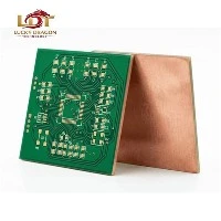


2 oz heavy copper PCB fabrication features a nominal copper weight of 70 um per square foot on designated layers, doubling standard 1 oz baselines. This increased thickness reduces conductor resistance, lowers thermal resistance, and accommodates high continuous currents without excessive localized heating. Fabricated using high-grade FR-4 (Tg >= 170°C) and specialized differential etching compensation, these boards balance fine-line capability with high-current power distribution on a single footprint.
Technical Specifications
|
Parameter |
Specification |
|
Base Material |
FR-4 (Tg 170°C / 180°C), Polyimide, Ceramic-filled PTFE |
|
Finished Copper Weight |
2 oz (Outer & Inner layers available) |
|
Minimum Trace Width / Spacing |
4 mil / 4 mil (for 2 oz copper via controlled plating/etching) |
|
Board Thickness |
0.4 mm to 3.2 mm |
|
Maximum Layer Count |
Up to 24 Layers |
|
Surface Finish |
ENIG, HASL (Lead-Free), Immersion Silver, OSP, Hard Gold |
|
Solder Mask |
Green, Black, Blue, Red, White (High-temperature LPI) |
|
Minimum Laser Hole Size |
0.1 mm (HDI structures) |
|
Impedance Control Tolerance |
+/- 5% |
Key Features
Elevated Current Carrying Capacity: Supports higher continuous and surge currents compared to standard 1 oz boards, minimizing trace width requirements for high-current power rails.
Thermal Dissipation: Thick copper planes act as efficient heat spreaders, transferring thermal energy away from high-power components (MOSFETs, IGBTs) to internal planes or external heatsinks.
Mechanical Robustness: Enhanced structural integrity at press-fit pin sites and screw-down mounting holes, resisting mechanical stress and thermal fatigue during assembly.
Controlled Etching Compensation: Proprietary line-width compensation prevents excessive undercutting during heavy copper etching, maintaining predictable trace impedance.
Applications
Power Electronics
Switch-mode power supplies (SMPS), DC-DC converters, and uninterruptible power supplies (UPS).
Automotive Systems
EV onboard chargers, motor drive inverters, and battery management systems (BMS).
Renewable Energy
Solar PV string inverters, wind turbine control systems, and energy storage system (ESS) power racks.
Industrial Automation
High-power servo drives, PLC output modules, and industrial welding equipment.
Customization
Asymmetric Copper Weights: Combine 2 oz power planes with 1 oz signal layers to optimize routing density and cost.
Stackup Engineering: Custom dielectric spacing and prepreg combinations engineered for specific differential impedance targets.
Thermal Vias Arrays: Staggered or filled/capped via arrays directly beneath high-dissipation thermal pads.
Specialized Coatings: Thick-film solder mask application to cover heavy traces securely without cracking or exposing copper edges.
Quality Control
AOI (Automated Optical Inspection): Inline optical scanning of inner and outer layers post-etching to detect shorts, opens, and line-width violations.
Flying Probe & Bed-of-Nails Testing: 100% electrical continuity and isolation testing executed on every production panel.
X-Ray Fluorescence (XRF): Non-destructive measurement of surface finish thickness (e.g., gold/nickel thickness verification).
Microsection Analysis: Destructive physical analysis performed per lot to verify copper thickness, barrel plating uniformity, and dielectric spacing.
Manufacturing & Certifications
Facility Capabilities
Cleanroom fabrication lines equipped with direct imaging (DI) systems, precision heavy-copper etching lines, and high-pressure lamination presses.
Management Standards
ISO 9001 (Quality Management), ISO 14001 (Environmental Management), and IATF 16949 (Automotive Quality Management).
Product Compliance
UL-certified (File E-number on record) and fully compliant with RoHS and REACH material directives.
Packaging & Delivery
Packaging Details: Vacuum-sealed anti-static ESD bags with desiccant packs, cushioned with corrugated interleaving sheets inside double-walled export cartons.
Logistics Support: Express air freight for prototype batches (3-5 day transit); consolidated sea/air freight for volume production. Traceable via major global forwarders.
FAQ
Q: What is the minimum trace width and spacing achievable with 2 oz heavy copper PCB fabrication?
A: We routinely achieve 4 mil trace width and 4 mil spacing on 2 oz outer layers by utilizing fine-line differential etching parameters and controlled acid flow rates.
Q: Can 2 oz copper be applied to inner layers of a multilayer thick copper printed circuit board?
A: Yes. Both inner and outer layers can be specified at 2 oz (or mixed, such as 2 oz inner and 1 oz outer) depending on your power distribution architecture.
Q: How do you prevent etching undercut on thick copper layers during high current PCB stackup production?
A: We apply proprietary compensation algorithms to Gerber files prior to photolithography, adjusting trace widths to account for lateral acid erosion during the extended etching cycle.
Q: What surface finish works best with 2 oz heavy copper boards carrying high current?
A: ENIG (Electroless Nickel Immersion Gold) is recommended for flat contact surfaces and wire bonding, while Immersion Silver or Lead-Free HASL are suitable for general power modules requiring robust solder joint intermetallic formation.
Q: What is the standard lead time for 2 oz heavy copper PCB prototypes?
A: Standard prototype fabrication takes 5 to 7 business days, depending on layer count and surface finish complexity. Expedited 3-day service is available upon review of Gerber data.
Q: Do you perform thermal stress testing on heavy copper batches?
A: Yes. Sample coupons from every production panel undergo thermal shock testing (solder float at 288°C for 10 seconds) to verify lamination integrity and resistance to delamination.
Request a Quote
Submit your Gerber files (RS-274X or ODB++), drill files, and fabrication drawing to our engineering team for rapid DFM evaluation.
Required Data: Layer stackup details, finished copper weight requirements, surface finish preference, and quantity.
Response Time: Quotations and DFM feedback delivered within 12 business hours.
Hot Tags: 2 oz heavy copper pcb, China 2 oz heavy copper pcb manufacturers, suppliers, factory


