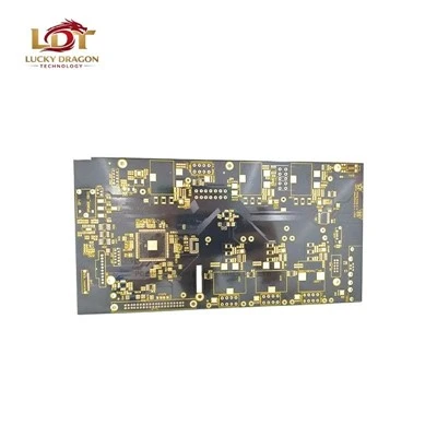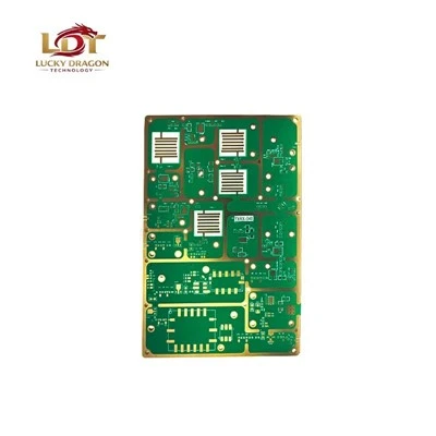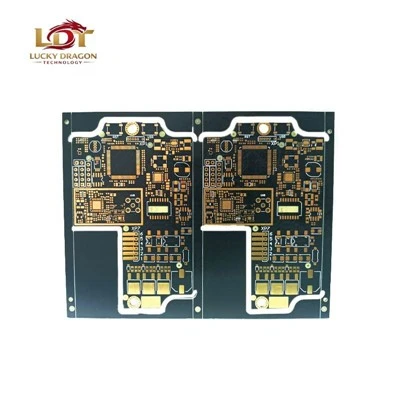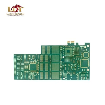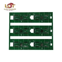
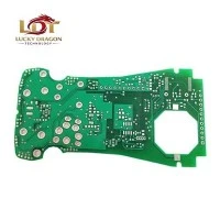

HDI Rigid-Flex PCBs integrate rigid FR4/polyimide board structures and flexible polyimide circuits into a single monolithic unit. By utilizing laser-drilled microvias, blind/buried vias, and fine-line etching, this architecture replaces traditional bulky wiring harnesses and board-to-board connectors. It reduces system volume and weight while eliminating failure points from vibration and mechanical stress in dynamic environments.
Technical Specifications
|
Parameter |
Standard Capability |
Advanced Capability |
|
Total Layer Count |
2 to 16 Layers |
Up to 30+ Layers |
|
Rigid / Flex Breakdown |
2L rigid + 1L flex up to 8L rigid + 4L flex |
Custom multi-layer flex configurations with air-gaps |
|
Min. Trace / Space (Line/Width) |
3.5 mil / 3.5 mil (0.09mm) |
2 mil / 2 mil (0.05mm) |
|
Min. Laser Microvia Size |
4 mil (0.1mm) |
3 mil (0.075mm) stacked/staggered |
|
Dielectric Materials |
Polyimide (Pyralux, 2AP/LF), FR4 (Tg 170C / 180C) |
Liquid Crystal Polymer (LCP), High-frequency laminates (Rogers) |
|
Surface Finish |
ENIG, Immersion Tin, OSP |
ENEPIG, Hard Gold, Selective Plating |
|
Impedance Tolerance |
+/-10 percent |
+/-5 percent (Time Domain Reflectometry verified) |
|
Max. Board Thickness Ratio |
Aspect ratio up to 10:1 (Rigid) |
Aspect ratio up to 12:1 |
Key Features
Zero-Connector Architecture
Direct soldered or integrated transitions remove mechanical mating interfaces prone to shock and vibration failure.
Controlled Z-Axis Interconnects
Laser microvias enable dense fan-out routing beneath fine-pitch BGAs (0.4mm pitch and below).
Dynamic Flex Endurance
Designed for continuous bending applications using adhesiveless polyimide copper-clad laminates.
Precise Impedance Routing
Strict dielectric thickness control and reference plane management maintain signal integrity up to 10 Gbps+.
Applications
Medical Equipment
Ultrasound probes, wearable patient monitors, and miniaturized endoscopic imaging modules.
Aerospace & Defense
Avionics flight control displays, helmet-mounted tracking systems, and radar telemetry units.
Industrial & Robotics
Robotic arm joint feedback loops, handheld rugged data collectors, and automated test fixtures.
Consumer Electronics
AR/VR optics assemblies, ultra-slim enterprise laptops, and high-density gimbal cameras.
Customization Options
Stiffener Integration: Polyimide (FR4), aluminum, or stainless-steel stiffeners added to component mounting zones or ZIF connector insertion edges.
Shielding Layers: Conductive silver paste, shielding film (Pyralux TK), or copper hatch layers applied for EMI/RFI suppression.
Coverlay / Solder Mask: Amber/black polyimide coverlays (thickness 0.5 mil to 2 mil) or liquid photoimageable (LPI) flexible solder masks.
PSA / Adhesives: Integration of 3M pressure-sensitive adhesives (PSA) on the underside of flex tails for structural mounting.
Quality Control & In-House Testing
AOI & Microsectioning: Automated Optical Inspection on inner/outer layers; destructive cross-section analysis per IPC-TM-650 to verify microvia barrel integrity and copper wall thickness.
Electrical Testing: Flying probe testing for prototypes; fixture-based bed-of-nails testing for volume production, combined with 4-wire Kelvin resistance checks.
Thermal Stress Screening: Solder float simulation (288C, 10 seconds) and thermal shock testing (-55C to +125C) to detect delamination risks.
Ionic Cleanliness Testing: Ion chromatography analysis ensuring ionic contaminant levels remain below 1.0 microgram/inch2 NaCl equivalent.
Manufacturing & Certifications
Facility Scale: 15,000 m2 cleanroom production plant equipped with Hitachi high-speed CNC drills, Orbotech direct imaging (LDI) systems, and Schmoll laser ablation units.
Process Traceability: Barcode tracking per individual panel from raw copper lamination to final electrical test.
Compliance Standards:
- ISO 9001:2015 (Quality Management System)
- IATF 16949:2016 (Automotive Quality Standard)
- ISO 13485:2016 (Medical Devices Quality Management)
- IPC-A-600 Class 3 / IPC-6013 Certified manufacturing lines
- RoHS and REACH compliant processing
Packaging & Delivery
Packaging Specification: Vacuum-sealed ESD-safe moisture barrier bags with silica gel packs and humidity indicator cards, packed in rigid double-wall corrugated cartons.
Logistics Partners: Direct air freight partnerships via DHL, FedEx, and UPS with expedited customs clearance documentation.
Lead Times:
- Standard Prototype: 7-12 working days (dependent on stack-up complexity)
- Volume Production: 15-25 working days
Frequently Asked Questions
Q: What is the minimum bend radius supported for dynamic flexing applications?
A: For dynamic flex applications, the general rule is 10x the total thickness of the flex section for adhesiveless double-sided circuits, and up to 20x for multi-layer flex sections. Static (one-time installation) bends permit a radius down to 6x the thickness.
Q: How do you prevent delamination at the rigid-flex transition zone during thermal reflow?
A: We incorporate staggered layer transitions, teardrop pads, anchored coverlay extensions into the rigid prepreg zone, and vacuum-assisted lamination parameters tailored for dissimilar coefficient of thermal expansion (CTE) materials.
Q: Can you handle impedance calculations if we supply raw stack-up constraints?
A: Yes. Our engineering team uses Polar Si8000 field solvers to simulate trace width, spacing, and reference plane parameters against your dielectric requirements prior to production sign-off.
Q: What file formats are required to initiate an Engineering Query (EQ) and RFQ?
A: Submit Gerber RS-274X or ODB++ fabrication data, an IPC-2581 compliant file package, a detailed drill drawing containing layer stack-up definitions, and a read-me text file specifying controlled impedance lines.
Q: Are blind and buried microvias filled with copper or resin?
A: Laser microvias are filled using sequential copper electroplating (via filling) to allow pad-via placement on BGA lands without solder wicking issues during assembly.
Q: What is your standard procedure if an open or short circuit is detected during electrical testing?
A: Defective panels are logged into our Corrective and Preventive Action (CAPA) tracking system. Root-cause isolation (etching residue, laser drilling offset, or plating voids) is performed before releasing a replacement lot.
Request a Quote & Engineering Resources
To receive a formal quotation within 24 hours, upload your Gerber/ODB++ package and stack-up specifications directly to our engineering portal or email your documentation package to our technical sales team.
Hot Tags: hdi rigid-flex pcb, China hdi rigid-flex pcb manufacturers, suppliers, factory