
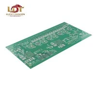
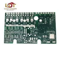

A 4-layer multilayer printed circuit board consists of two outer copper layers and two internal layers-typically designated as continuous power and ground planes-bonded together by prepreg under high temperature and vacuum pressure. This architecture increases routing density, reduces electromagnetic interference (EMI), and maintains signal integrity for compact electronic hardware.
- Supplied as bare boards for surface-mount (SMT) or through-hole (THT) assembly.
- Validated through 100% automated electrical netlist testing prior to vacuum packaging.
Technical Specifications
Note: Standard production capabilities. Custom configurations require engineering review.
|
Parameter |
Specification Range |
Standard Tolerance |
|
Layer Count |
4 Layers |
N/A |
|
Finished Board Thickness |
0.4mm – 3.2mm |
+/-10% |
|
Base Material (Laminate) |
FR-4 (Tg 130C, 150C, 170C), High-Tg FR-4, Aluminum-backed (hybrid) |
IPC-4101 compliant |
|
Copper Weight |
Outer: 1 oz (35um) to 3 oz (105um) Inner: 0.5 oz (18um) to 2 oz (70um) |
IPC-A-600 Class 2 / Class 3 |
|
Min. Trace Width / Spacing |
3.5 mil / 3.5 mil (0.09mm) |
+/-20% |
|
Min. Finished Hole Size |
0.15mm (Mechanical), 0.10mm (Laser via capability) |
+/-0.025mm |
|
Surface Finish |
ENIG, HASL (Lead-free), OSP, Immersion Silver, Immersion Tin |
IPC-PL-011 |
|
Solder Mask Color |
Green, Black, Matte Black, Blue, Red, White, Yellow |
Visual inspection per IPC |
|
Impedance Control Tolerance |
+/-10% (TDR tested) |
Engineering simulation required |
Key Features
Internal Power/Ground Planes
Lowers ground impedance and stabilizes DC power distribution to sensitive ICs.
Controlled Electromagnetic Interference (EMI)
Dedicated internal planes shield high-frequency signals and reduce loop areas.
High-Density Routing
Accommodates fine-pitch BGAs and complex surface-mount components without increasing board footprint.
Thermal Management
Distributes heat evenly across internal copper planes, preventing localized thermal stress.
Applications
Industrial Automation
PLC controllers, motor drives, and industrial human-machine interfaces (HMIs).
Automotive Electronics
Infotainment sub-modules, LED lighting controllers, and sensor interfaces (non-safety-critical).
IoT & Telecommunications
Wi-Fi/cellular routers, gateway controllers, and edge computing nodes.
Medical Equipment
Patient monitors, diagnostic benchtop units, and laboratory testing devices.
Customization
Engineering support is available for custom stack-up design, impedance modeling, and material selection.
Stack-up Optimization: Customized dielectric thickness between layers to achieve target differential/single-ended impedance (50 ohm, 100 ohm).
Special Processes: Blind/buried vias, peelable solder mask, carbon ink jumpers, and edge plating.
Panelization: Customized array layouts (V-score or tab-route) optimized for pick-and-place assembly machines.
Quality Control & Laboratory Verification
Manufacturing follows IPC-A-600 standards. Every production panel undergoes multi-stage inspection:
AOI (Automated Optical Inspection): Detects open circuits, short circuits, etching defects, and copper residue on inner and outer layers prior to lamination.
X-Ray Registration Inspection: Verifies core-to-core alignment and drill registration accuracy prior to outer layer imaging.
100% Electrical Netlist Testing: Executed via Flying Probe Testers (for prototypes/NPI) or Bed-of-Nails fixtures (for volume production).
In-House Laboratory Analysis: Coupon testing for microsection analysis (verifying copper wall thickness and barrel integrity) and solderability testing per J-STD-003.
Manufacturing & Facility Capabilities
Production Floor Equipment: Equipped with direct imaging (DI) exposure systems, high-speed CNC drilling centers, multi-opening vacuum lamination presses, and horizontal electroplating lines ensuring uniform copper deposition.
Traceability: Lot-level material tracking utilizing laser-etched matrix codes on panel borders.
Certifications: ISO 9001:2015, IATF 16949 (Automotive Quality Management), ISO 14001, and UL-listed (E-number available upon request). Fully RoHS and REACH compliant.
Packaging & Delivery
Packaging: Vacuum-sealed anti-static ESD bags with desiccants and shock-absorbent bubble wrap. Heavy-duty double-wall corrugated cartons reinforced for international export freight.
Logistics Support: Express air freight for urgent prototypes (3 to 5 days transit) and sea/air freight consolidation for scheduled volume shipments.
FAQ
Q: What file formats are required to initiate production?
A: Gerber RS-274X file format along with an IPC-D-356 netlist and a fabrication drawing specifying board thickness, copper weight, and surface finish.
Q: How do you handle impedance-controlled 4-layer designs?
A: Submit your target impedance values and stack-up requirements. Our engineering team simulates trace width and dielectric spacing using Polar software before production release.
Q: What is the standard turnaround time for 4-layer prototypes?
A: Standard prototype fabrication takes 3 to 5 business days, subject to material availability and design complexity.
Q: Do you perform 100% electrical testing before shipment?
A: Yes, every single bare board is electrically tested against the original netlist file prior to vacuum packaging.
Request a Quote
Submit your Gerber files and technical specifications for an engineering review and quotation:
- Board dimensions and quantity
- Layer count and finished board thickness
- Surface finish and solder mask color
- Target delivery schedule and shipping destination
Hot Tags: 4-layer multilayer pcb, China 4-layer multilayer pcb manufacturers, suppliers, factory


