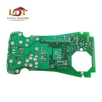

The 6-layer multilayer PCB provides an optimized routing architecture for dense circuit designs requiring dedicated internal power and ground planes. By separating signal routing from power distribution, this stackup configuration suppresses electromagnetic interference (EMI) and maintains controlled impedance for high-speed digital signals. Standard configurations utilize FR-4 glass-epoxy substrates, supporting complex layouts for industrial controls, telecommunications hardware, and automotive electronic control units (ECUs).
Technical Specifications & Stackup Architecture
|
Parameter |
Standard Capability |
Advanced Capability |
|
Layer Count |
6 Layers |
6 Layers |
|
Board Thickness |
1.6 mm |
0.4 mm - 3.2 mm |
|
Thickness Tolerance |
+/- 10% |
+/- 5% |
|
Copper Weight (Outer) |
1 oz (35 um) |
0.5 oz - 3 oz |
|
Copper Weight (Inner) |
0.5 oz (17 um) |
1 oz - 2 oz |
|
Min. Trace Width / Spacing |
4 mil / 4 mil |
3 mil / 3 mil |
|
Min. Laser Drill Hole Size |
0.2 mm (Mechanical) |
0.1 mm (Laser via) |
|
Impedance Tolerance |
+/- 10% |
+/- 5% |
|
Surface Finish |
ENIG, HASL (Lead-Free), OSP |
Immersion Silver, Immersion Tin, Hard Gold |
|
Solder Mask Color |
Green |
Black, Blue, Red, Yellow, White, Purple |
|
Max Board Dimension |
500 mm x 600 mm |
Customizable per panel layout |
Key Features
Dedicated Internal Planes: Two internal ground/power planes isolate signal layers, reducing cross-talk and providing stable reference planes for controlled impedance routing.
Via Architecture Support: Accommodates through-hole, blind, and buried vias to optimize routing density on high-pin-count BGA components.
Thermal Management: Internal copper planes act as thermal heat spreaders, dissipating localized heat generated by power regulators and high-current processors.
Stackup Flexibility: Symmetrical dielectric spacing prevents board warpage during thermal reflow cycles.
Applications
Industrial Automation: Programmable Logic Controllers (PLCs), motor drives, and factory automation sensor nodes.
Telecommunications: Network routers, optical transceivers, and base station interface cards.
Automotive Systems: Dashboard instrument clusters, Advanced Driver Assistance Systems (ADAS) sensor modules, and battery management systems (BMS).
Medical Equipment: Patient monitoring hardware, diagnostic imaging controllers, and portable therapeutic devices.
Customization & Engineering Support
Free DFM Check: Engineering review of Gerber RS-274X, ODB++, and IPC-2581 data packages to resolve design-rule conflicts, acid traps, and drill-to-copper violations before tooling.
Impedance Modeling: Calculations performed using Polar SI8000 software to verify target trace widths and dielectric parameters prior to production.
Material Selection: Options include high-Tg FR-4 (Tg >= 170 deg C or 180 deg C), halogen-free laminates, and high-frequency PTFE/ceramic-filled substrates (e.g., Rogers series) for RF integration.
Specialized Processing: Peelable solder masks, carbon ink jumpers, edge plating, and countersunk mounting holes.
Quality Control & Testing
Incoming Material Inspection: X-ray fluorescence (XRF) testing verifies copper foil thickness and laminate resin content.
Automated Optical Inspection (AOI): Inline optical scanning detects etching defects, shorts, and opens on inner and outer layers post-etching.
Electrical Testing: 100% flying probe testing or fixture-based bed-of-nails testing validates netlist connectivity at test voltages up to 250V.
Impedance Verification: Time-Domain Reflectometry (TDR) test coupons evaluated on every production panel to confirm target differential and single-ended impedance values.
Microsection Analysis: Destructive physical analysis performed per IPC-TM-650 to inspect plating thickness, barrel fill, and thermal stress resistance.
Manufacturing & Certifications
Production Infrastructure
Fully automated LDI (Laser Direct Imaging) exposure systems, vacuum lamination presses, and direct-plating chemical lines ensure consistent trace geometry and interlayer registration within +/- 15 um.
Quality & Environmental Standards
- ISO 9001:2015 Quality Management System
- IATF 16949 Automotive Quality Management
- ISO 14001 Environmental Management
- UL Certification (E-File compliance for flammability rating 94V-0)
- IPC-A-600 Class 2 / Class 3 compliance
Packaging & Delivery
Packaging Specifications: Vacuum-sealed anti-static bags containing desiccant packs, layered with moisture barrier aluminum foil wrapping and corrugated cardboard cushioning to prevent transit damage or oxidation.
Logistics Options: Air freight, express courier, and ocean freight shipping options paired with commercial invoice and packing list documentation for international customs clearance.
FAQ
Q: What file formats are required for 6-layer PCB fabrication?
A: Gerber RS-274X files alongside an NC drill file, plus a text file detailing layer stackup sequence, finished board thickness, and copper weight specifications. ODB++ formats are also fully supported.
Q: How do you handle controlled impedance stackup design?
A: Engineering teams utilize Polar SI8000 software to calculate required trace widths and dielectric thicknesses based on designated dielectric constants (DK) of the specified laminate material. Stackup reports are sent for client approval prior to production.
Q: What is the standard lead time for prototype versus production orders?
A: Standard prototype fabrication requires 5 to 7 business days. Batch production runs typically require 10 to 15 business days, depending on board complexity and surface finish selection. Expedited options are available upon request.
Q: Are boards tested before shipment?
A: Yes. Every manufactured panel undergoes 100% electrical continuity and isolation testing via flying probe or dedicated test fixtures, alongside visual inspection and microsection coupon analysis.
Request a Quote
Submit your Gerber files and fabrication drawings to engineering for a complimentary DFM review and formal quotation.
Required Data: Gerber files, drill files, layer stackup drawing, and quantity requirements.
Response Time: Quotations and initial DFM feedback returned within 24 business hours.
Hot Tags: 6-layer multilayer pcb, China 6-layer multilayer pcb manufacturers, suppliers, factory