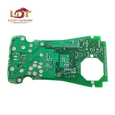
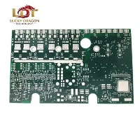

The 8-layer multilayer PCB configuration routes complex high-speed signals, dense power distribution, and dedicated ground planes within a rigid structure. Standard construction alternates four signal routing layers with two internal power planes and two solid ground planes to suppress electromagnetic interference (EMI) and cross-talk. Fabricated to IPC-A-600 Class 2/3 specifications, supporting controlled impedance tolerances within +/-10% for high-frequency data transmission. Seamlessly scalable from quick-turn prototype runs to volume production.
Technical Specifications
|
Parameter |
Specification Standard |
|
Layer Count |
8 Layers (4 Signal Routing, 2 Power Planes, 2 Ground Planes) |
|
Board Thickness |
1.6 mm standard (Range: 0.8 mm – 3.2 mm) |
|
Min. Trace Width / Spacing |
3.5 mil / 3.5 mil (0.09 mm / 0.09 mm) |
|
Min. Finished Hole Size |
0.2 mm (Mechanical drill), 0.1 mm (Laser drilled microvia) |
|
Base Material |
FR-4 (Tg >= 170°C, Dk approx. 4.4), High-frequency laminates (Rogers RO4000 series) |
|
Copper Weight |
Outer layers: 1 oz (35 micrometers) / Inner layers: 0.5 oz or 1 oz |
|
Surface Finish |
ENIG, HASL-Lead Free, OSP, Immersion Silver, Immersion Tin |
|
Solder Mask / Silkscreen |
Green, Black, Blue, Red, Matte Black, White / White, Yellow |
|
Impedance Tolerance |
+/-10% (Single-ended 50 ohms, Differential pairs 100 ohms) |
|
Max. Panel Size |
500 mm x 600 mm |
Key Features
Dedicated Internal Planes: Two solid copper planes dedicated to power and ground distribution reduce loop areas and stabilize power integrity.
Controlled Impedance Architecture: Dielectric thickness and trace widths are calculated via Polar Si8000 software to ensure strict signal integrity matching across high-speed channels.
Microvia & HDI Support: Accommodates blind and buried via structures for dense BGA component fan-outs and high pin-count IC packaging.
Thermal Endurance: High-Tg FR-4 material prevents resin degradation during multiple lead-free reflow cycles (IPC-TM-650 thermal stress tested at 288°C for 10 seconds).
Applications
Industrial Automation
Programmable Logic Controllers (PLCs), high-speed servo drives, and industrial sensor hubs.
Telecommunications
5G sub-6 GHz infrastructure units, high-capacity network routers, and data switches.
Automotive Electronics
Advanced Driver Assistance Systems (ADAS) processing units and Electric Vehicle (EV) power distribution modules.
Medical Equipment
Patient telemetry monitors, portable ultrasound systems, and medical imaging interfaces.
Customization & Volume Flexibility
Minimum Order Quantity (MOQ): Flexible prototyping starting from 5 pieces, scaling up to 10,000+ units for volume manufacturing with tiered pricing structures.
Stack-Up Engineering: Custom asymmetrical or symmetrical stack-up design based on your Altium, Cadence Allegro, or KiCad Gerber and ODB++ outputs.
Material Alternatives: Select between standard high-Tg FR-4, halogen-free laminates, or hybrid PTFE/FR-4 stacks for low-loss high-frequency requirements.
Advanced Processing: Edge plating, countersink/counterbore holes, peelable solder mask, and carbon ink jumpers.
Quality Control & Inspection
Every production panel is verified through rigorous multi-stage inspection:
Electrical Testing: 100% flying probe test or dedicated fixture testing at 250V–300V to guarantee zero opens or shorts.
Automated Optical Inspection (AOI): Multi-axis scanning of inner and outer layers post-etching to catch trace anomalies and etching defects early.
Impedance Verification: Panel-specific test coupons measured using Time-Domain Reflectometry (TDR) to validate dielectric performance.
Micro-Section Analysis: Destructive physical cross-sectioning per production batch to verify plated through-hole (PTH) copper wall thickness and resin fill.
Manufacturing Capabilities & Certifications
Production Line Tech: Direct Laser Imaging (LDI) exposure systems, vacuum multi-layer lamination presses, and high-speed CNC routing machinery.
Full Traceability: Unique barcode serialization etched onto every panel, tracking material lots, processing shifts, and QC logs.
Certifications:
- ISO 9001:2015 Quality Management System
- IATF 16949 Automotive Quality System
- ISO 14001 Environmental Management System
- UL File Number: E480000 (UL 94V-0 Flammability Rating)
- RoHS and REACH Directives Compliant
Packaging & Logistics
Packaging Standards: Vacuum-sealed anti-static shielding bags with desiccant packs, cushioned with corrugated interleaving sheets to prevent board flex and moisture ingress during transit.
Carton Labeling: Outer packaging explicitly labeled with part numbers, revision levels, batch codes, and manufactured quantities.
Shipping Channels: Express air freight (DHL, FedEx, UPS) for rapid prototype delivery (3–5 days) and scheduled air/ocean freight for volume batches.
FAQ
Q: What file formats are required to initiate manufacturing?
A: Gerber RS-274X, ODB++ manufacturing datasets, and a comprehensive fabrication drawing outlining stack-up details, impedance targets, and surface finish requirements.
Q: Do you offer a pre-production DFM review?
A: Yes. Our engineering team conducts a thorough Design for Manufacturability (DFM) check upon file submission, flagging potential etch traps, acid traps, or via-to-trace clearance issues prior to tooling.
Q: How are impedance discrepancies handled before pressing?
A: Our engineers review your stack-up against actual dielectric prepreg availability. If adjustments are needed to compensate for resin flow and copper etching loss, we coordinate with your layout team prior to production.
Q: What is the typical lead time for an 8-layer prototype?
A: Standard prototype fabrication takes 5 to 7 business days from engineering sign-off. Expedited 4-day turnaround options are available.
Q: Are test coupons provided with shipments?
A: Yes, micro-section coupons and TDR impedance test coupons can be included from the panel border upon request.
Request a Quote & DFM Review
Submit your Gerber or ODB++ data for a complimentary DFM evaluation and a formal quotation delivered within 24 hours.
Email: sales@Ldtac.com
Submission Checklist: Gerber data, drill files, README text file detailing material types, copper weights, and surface finish.
Hot Tags: 8-layer multilayer pcb, China 8-layer multilayer pcb manufacturers, suppliers, factory