
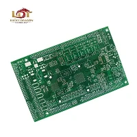
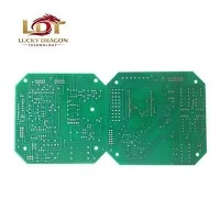

The 2+N+2 HDI PCB utilizes a sequential lamination structure comprising two layers of laser-drilled microvias on both the top and bottom sides of a central multi-layer core (N layers). This architecture delivers high routing density and signal integrity for space-constrained, high-frequency electronic assemblies.
Fab capabilities support fine-line etching and staggered/stacked microvia configurations to route dense BGAs (pitch down to 0.4 mm or lower) while maintaining controlled impedance and structural integrity. Upload Gerber/ODB++ and stack-up files for a 24-hour DFM and impedance feasibility check.
Technical Specifications
|
Parameter |
Specification Range |
|
Stack-up Structure |
2+N+2 HDI (Sequential Lamination) |
|
Layer Count (N Core) |
2 to 12 layers (Customizable) |
|
Min. Trace / Space (Line/Width) |
2.5 mil / 2.5 mil (0.063 mm / 0.063 mm) |
|
Min. Laser Drill Hole Size |
3 mil (0.075 mm) |
|
Min. Mechanical Hole Size |
6 mil (0.15 mm) |
|
Finished Board Thickness |
0.8 mm - 3.2 mm |
|
Impedance Tolerance |
+/- 10% (Standard), +/- 5% (Strict) |
|
Aspect Ratio (Microvia) |
1:1 |
|
Aspect Ratio (Mechanical) |
Up to 12:1 |
|
Surface Finishes |
ENIG, Immersion Silver, OSP, ENEPIG, Hard Gold |
|
Base Materials |
FR-4 (High-Tg >= 170 deg C), Isola (FR408HR, Astra MT77), Panasonic (Megtron 6/7) |
Key Features
Sequential Build-up Technology: Enables laser microvias (<= 0.1 mm) on outer layers, freeing up internal routing channels for power and ground planes.
Via-in-Pad Capability: Plates copper directly over filled microvias, reducing parasitic inductance and saving layout surface area under fine-pitch BGAs.
Controlled Impedance Performance: Precise dielectric thickness management and etching compensation achieve +/- 5% differential impedance control for high-speed differential pairs (PCIe Gen 4/5, Ethernet 100G).
High Thermal Reliability: Uses high-Tg (170 deg C to 210 deg C) laminates and copper-filled conductive pastes, passing IST (Interconnect Stress Testing) and thermal cycling per IPC-TM-650.
Applications
Telecommunications
5G active antenna units (AAU), optical transceivers, and high-speed routers.
Automotive Electronics
ADAS processing units, LiDAR interface boards, and infotainment domain controllers.
Industrial & Medical
Ultrasound diagnostic equipment, high-frequency industrial controllers, and defense telemetry systems.
Computing
High-performance peripheral cards and embedded server motherboards.
Customization
Dielectric Materials: Selectable standard FR4, low-loss, or ultra-low-loss laminates based on signal frequency and dielectric constant (Dk <= 3.8, Df <= 0.004).
Copper Weight: Outer layers 0.5 oz to 2 oz; inner layers 0.5 oz to 3 oz.
Solder Mask & Legend: Green, black, blue, red, white, or yellow liquid photoimageable (LPI) solder mask.
Surface Treatment Options:
- ENIG: 2 - 5 uin Au over 120 - 240 uin Ni.
- Immersion Silver: 8 - 15 uin.
- ENEPIG: For wire bonding and multiple reflow cycles.
Quality Control
Manufacturing processes operate under ISO 9001 and IATF 16949 guidelines, backed by rigorous metrology and test routines:
AOI (Automatic Optical Inspection): 100% inspection of inner and outer layers for etch defects, opens, and shorts.
X-Ray Inspection: Verifies core layer-to-layer alignment and sequential lamination registration.
Flying Probe & Fixture Testing: 100% electrical continuity and isolation testing (test voltage up to 250V).
Microsection Analysis: Destructive physical analysis (DPA) on production coupons to measure copper wrap, via barrel thickness, and dielectric spacing.
TDR (Time Domain Reflectometry): Coupon-based impedance verification prior to shipment.
Manufacturing & Certifications
Production Facilities: Cleanroom fabrication plant equipped with direct imaging (DI) systems, high-precision CO2/UV laser drilling machines, vacuum lamination presses, and horizontal plating lines.
Certifications:
- ISO 9001:2015 Quality Management System
- IATF 16949 Automotive Quality Management
- ISO 14001 Environmental Management System
- UL Certified (E-File matching IPC standards)
- RoHS and REACH compliant materials
Packaging & Delivery
Packaging: Vacuum-sealed anti-static ESD bags with desiccant packs, interleaved with shock-absorbing foam inside double-wall corrugated export cartons. Moisture-barrier bagging (MBB) and Humidity Indicator Cards (HIC) provided for sensitive high-frequency boards.
Logistics: Shipped via air freight (DHL, FedEx, UPS) or sea freight. Standard delivery includes full shipping documentation, Certificate of Analysis (CoA), and microsection test reports.
FAQ
Q: What is the minimum laser via and mechanical drill size you can fabricate for 2+N+2 structures?
A: Laser microvias are fabricated down to 3 mil (0.075 mm), and mechanical drill holes down to 6 mil (0.15 mm). Aspect ratio for microvias is maintained at 1:1.
Q: Can you handle blind and buried via filling with copper plating?
A: Yes. Microvias in the 2+N+2 stack-up undergo direct copper filling, planarization, and over-plating to allow via-in-pad design implementations.
Q: What Gerber and CAD data formats are required for DFM review?
A: Gerber RS-274X or ODB++ format, paired with an NC drill file, IPC-D-356 netlist, and a stack-up drawing specifying target impedance values for designated traces.
Q: How do you verify impedance control on production panels?
A: Test coupons are etched on the same manufacturing panel alongside the production boards. Impedance is verified using Time Domain Reflectometry (TDR) testing, and test reports are included with delivery.
Q: What is the standard production lead time for 2+N+2 HDI prototypes vs. volume production?
A: Prototype fabrication takes 7 to 10 working days upon DFM approval. Mass production lead time ranges from 15 to 25 working days depending on layer count, volume, and material availability.
Q: Which IPC standard do your acceptance criteria follow?
A: All printed circuit boards are manufactured and inspected in accordance with IPC-A-600 Class 2 or Class 3 standards, per customer specification requirements.
Request a Quote
Upload your Gerber files, stack-up requirements, and volume forecasts to receive a technical DFM review and quotation within 24 hours.
Hot Tags: 2+n+2 hdi pcb, China 2+n+2 hdi pcb manufacturers, suppliers, factory


