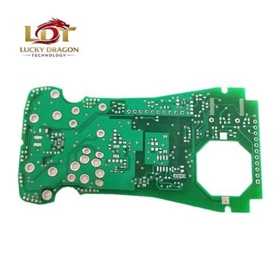

High-layer-count multilayer PCBs integrate 10 to 40+ conductive copper layers interspersed with dielectric prepreg. Designed for routing high-density signals and managing complex power distribution networks, these boards support rigorous electrical and thermal demands in dense electronic assemblies. Fabrication relies on strict registration control, sequential lamination management, and controlled-depth drilling to maintain signal integrity across deep-stack architectures.
Technical Specifications
|
Parameter |
Specification Range |
|
Layer Count |
10 to 40+ layers |
|
Board Thickness |
1.0 mm to 6.0 mm (Max Aspect Ratio 18:1) |
|
Min. Trace Width / Space |
3.0 mil / 3.0 mil (0.075 mm / 0.075 mm) |
|
Min. Laser Drill Hole Size |
4 mil (0.1 mm) |
|
Base Materials |
High-Tg FR-4 (Tg >= 170 deg. C), Megtron 6, Rogers RO4000 series, Isola |
|
Surface Finishes |
ENIG, Immersion Silver, HASL (Lead-free), OSP, Hard Gold |
|
Max. Board Size |
600 mm x 500 mm |
|
IPC Standard |
IPC-6012 Class 2 / Class 3 / Class 3/A |
Key Features
Controlled Impedance Precision: Tight trace width and dielectric thickness tolerance (+/- 5 percent) backed by internal field-solver modeling to minimize signal reflection and attenuation.
Advanced Via Structures: Support for sequential lamination blind vias, buried vias, stacked vias, and via-in-pad architectures to optimize routing density and grounding paths.
Dimensional Stability Control: Low-Z-axis expansion prepregs combined with optimized sequential pressing cycles to prevent inner-layer shifting and barrel cracking during thermal stress.
Thermal Management Integration: Accommodation for heavy copper inner planes (2 oz to 4 oz) and thermal vias to dissipate localized heat from high-power components.
Applications
Telecommunications
5G base station routers, optical transport networks, and core network switches.
Data Centers & Computing
High-performance servers, blade servers, and networking backplanes.
Medical Equipment
MRI controllers, CT scanner data acquisition units, and patient monitoring systems.
Aerospace & Defense
Avionics navigation systems, radar processors, and satellite communication modules.
Customization
Production adapts to custom stack-up designs provided via Gerber or ODB++ manufacturing files. CAM engineering performs stack-up symmetry and resin-flow simulations prior to tooling release to neutralize board warping risks during thermal cycles. Material substitution (e.g., swapping standard FR-4 for low-loss laminates like Megtron 6) is executed based on specified dielectric constant (Dk) and dissipation factor (Df) targets, accompanied by complete impedance simulation reports.
Quality Control
Pre-Production DFM Review: Senior CAM engineers execute rigorous drill-to-copper clearance, acid trap, and stack-up symmetry checks before tooling release to flag fabrication risks early.
AOI (Automated Optical Inspection): 100% inner-layer inspection for open circuits, shorts, and line width anomalies before lamination.
X-Ray Inspection: Real-time verification of layer-to-layer alignment and drill breakout prevention on multi-layer stacks.
Flying Probe & Bed-of-Nails Testing: Electrical continuity and isolation testing performed per netlist.
Microsection Analysis: Destructive physical analysis on test coupons per production lot to verify copper plating thickness, via wall integrity, and solder mask thickness.
Manufacturing & Certifications
In-house fabrication utilizes direct laser imaging (DI) systems, multi-opening vacuum lamination presses, and high-precision CNC mechanical/laser drills. Shop-floor operations maintain lot-level traceability of chemical baths and raw material batches to ensure consistent yields on high-density builds.
Quality Management: ISO 9001:2015, IATF 16949
Environmental Compliance: ISO 14001, RoHS, REACH
Product Certification: UL listed (E-file available upon request)
Packaging & Delivery
Packaging: Vacuum-sealed anti-static bags containing desiccant and humidity indicator cards, packed inside reinforced double-wall corrugated cartons. Moisture Barrier Bags (MBB) used for IPC/JEDEC J-STD-033 compliance on sensitive laminates.
Lead Time:
- Prototyping (10–16 layers): 7 to 10 working days.
- Batch Production (10–32 layers): 15 to 25 working days.
Logistics: Shipped via air freight or international courier with traceable tracking numbers.
FAQ
Q: What is the maximum layer count and aspect ratio you can reliably produce?
A: Fabrication handles up to 40 layers with a maximum aspect ratio of 18:1 for through-hole plating, and up to 3+N+3 HDI structures.
Q: How do you prevent board warping on high-layer-count panels with asymmetrical copper distribution?
A: Engineering performs stack-up balancing simulations before production. Copper foil distribution is balanced across inner layers, and symmetrical prepreg weaving styles are enforced during lamination to neutralize internal stress.
Q: Can you handle controlled impedance modeling based on our stack-up requirements?
A: Yes. Field solvers calculate trace widths and spacing against dielectric constants provided in material datasheets, returning an impedance report for approval prior to film generation.
Q: What test coupons are included with high-layer-count shipments?
A: Standard delivery includes IPC-compliant interconnect stress testing (IST) coupons or microsection coupons per manufacturing lot upon request.
Q: What is your minimum batch size for custom high-layer-count boards?
A: Prototyping orders start at 1 piece, with volume production scaling up to medium batches per release schedule.
Q: What file formats are required to initiate an RFQ?
A: Gerber RS-274X, ODB++ format, accompanied by an IPC netlist and an explicit fabrication drawing detailing stack-up, impedance requirements, and surface finish.
Request a Quote
Submit Gerber or ODB++ files along with layer count, board thickness, surface finish, and quantity requirements to receive a formal quotation and DFM review within 24 hours.
Hot Tags: high-layer-count multilayer pcb, China high-layer-count multilayer pcb manufacturers, suppliers, factory