
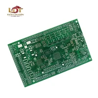
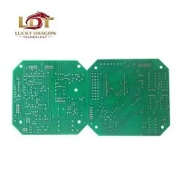

The 1+N+1 HDI PCB architecture integrates laser-drilled microvias on external layers bonded to a central multi-layer core (N), achieving high component density and fine-line routing capabilities beyond standard through-hole limitations. This configuration accommodates fine-pitch BGAs down to 0.4 mm pitch while preserving internal power and ground planes. Fabrication utilizes laser direct imaging (LDI), controlled-depth laser drilling, and sequential lamination processes tailored for high-density signal distribution, fully compliant with RoHS and REACH environmental directives.
Technical Specifications
|
Parameter |
Specification Limit |
|
Layer Count |
3 to 12 layers (1+N+1 stack-up) |
|
Min. Trace Width / Spacing |
3.0 / 3.0 mil (0.075 mm / 0.075 mm) |
|
Min. Laser Microvia Diameter |
4 mil (0.1 mm) |
|
Board Thickness Range |
0.6 mm - 2.4 mm |
|
Aspect Ratio (Microvia) |
Up to 1:1 |
|
Aspect Ratio (Through-Hole) |
Up to 12:1 |
|
Core Material Options |
FR-4 (Tg 170°C / 180°C), High-Frequency (Rogers, Taconic), Low-Loss (Panasonic Megtron 6/7) |
|
Surface Finish |
ENIG, Immersion Silver, OSP, HASL (Lead-Free), ENEPIG |
|
Solder Mask Color |
Green, Black, Blue, Red, White, Yellow (Matte/Glossy available) |
|
Impedance Control Tolerance |
±10% standard (±5% available upon request) |
Key Features
Sequential Lamination Processing: Eliminates mechanical drill stub resonance by stacking laser microvias directly over buried vias (stacked-via technology).
Fine-Pitch BGA Routing: Supports component pitches down to 0.4 mm without sacrificing power delivery plane integrity.
Controlled Dielectric Spacing: Maintains precise distance between reference planes and signal traces to suppress electromagnetic interference (EMI).
High-Tg Material Substrates: Withstands multiple thermal excursions during lead-free assembly reflow profiles up to 260°C.
Applications
5G Infrastructure
Active antenna units (AAU) and baseband radio units requiring high-frequency signal routing.
Automotive Electronics
Advanced Driver Assistance Systems (ADAS) radar modules and camera control units.
Industrial Computing
High-speed data acquisition boards and embedded edge processors.
Medical Equipment
Ultrasound imaging probes and portable diagnostic monitors requiring compact footprints.
Customization
Stack-Up Engineering: Engineering review of customer Gerber and stack-up proposals to optimize impedance and reduce layer count.
Material Substitution: Cross-referencing alternative laminate materials (e.g., Isola, Shengyi) to meet target cost and dielectric constant (Dk) requirements.
Plugged Via Options: Resin plugging (IPC-4761 Type VII) and copper plating over filled vias for pad-in-via applications.
Profiling Tolerances: Routing, V-scoring, and laser routing tailored to complex chassis enclosures.
Quality Control
Automated Optical Inspection (AOI): 100% inspection of inner and outer layers for etch defects, shorts, and opens.
Automated X-Ray Inspection (AXI): Verifies alignment and void percentages in stacked microvia structures.
Flying Probe Testing: Electrical continuity and isolation testing executed on 100% of fabricated panels prior to shipment.
Microsection Analysis: Destructive physical analysis performed per lot to verify copper plating thickness, dielectric thickness, and barrel crack resistance.
Manufacturing & Certifications
Facility Equipment Base: Equipped with Orbotech LDI systems, Hitachi high-speed CNC drilling machines, Schmoll laser via drills, and automatic vacuum lamination presses.
Process Capability: Cleanroom class 10,000 environment for dry film imaging and solder mask application.
Compliance Standards: Manufactured in accordance with IPC-A-600 Class 2/3 and IPC-6012 standards, meeting global RoHS and REACH regulatory requirements.
System Certifications: ISO 9001:2015, IATF 16949 (Automotive), ISO 13485 (Medical Devices), and UL certified (E-number tracking available on request).
Packaging & Delivery
Packaging Details
Vacuum-sealed ESD-safe moisture barrier bags containing silica gel and humidity indicator cards (HIC), packed in rigid double-wall corrugated cartons.
Logistics Partners
Expedited air freight via DHL, FedEx, and UPS for prototypes; palletized ocean or air freight for volume production batches.
Lead Times & Scaling
Prototypes (1+N+1): 5 - 7 business days with optimized panel utilization for quick-turn validation.
Volume Production: 12 - 18 business days, featuring tooling continuity to ensure seamless scaling from prototype batches to mass-production lines.
FAQ
Q: What is the minimum blind via size supported in a 1+N+1 configuration?
A: The standard production capability supports a minimum laser-drilled microvia diameter of 4 mil (0.1 mm) with a target capture pad size of 10 mil.
Q: Can you process customer-specified impedance calculations?
A: Engineering performs a DFM review using Polar Instruments SI8000/9000 software based on your dielectric constants and trace geometry before production release.
Q: What is the maximum copper thickness achievable on microvia layers?
A: Outer layers standardly support 1 oz finished copper after plating, with 0.5 oz and 2 oz options available subject to line/space limitations.
Q: How do you handle stacked-via reliability during thermal shock?
A: Controlled copper plating parameters fill microvias completely, and resin filling is applied where flat pad-in-via surfaces are required to prevent dimpling and solder joint voids.
Q: What documentation is provided with each delivery shipment?
A: Every batch includes a standard Certificate of Compliance (CoC), microsection test reports, electrical test verification records, and material traceability logs confirming RoHS and REACH compliance.
Q: What file formats are required to initiate a DFM check?
A: Gerber RS-274X or ODB++ files along with an IPC-D-356 netlist and a fabrication drawing specifying stack-up requirements.
Request a Quote
Submit Gerber files, stack-up requirements, and estimated annual volume to receive a DFM review and formal quotation within 24 hours.
Email: sales@Ldtac.com
Upload Portal: Secure DFM File Transfer Link
Hot Tags: 1+n+1 hdi pcb, China 1+n+1 hdi pcb manufacturers, suppliers, factory


