
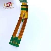
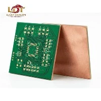

3 oz Heavy Copper PCBs feature a finished copper weight of 105 um per layer, engineered for high-current distribution and thermal management. By integrating thick copper into inner and outer layers, these boards handle high continuous current without excessive thermal accumulation, replacing bulky external busbars and reducing overall system footprint in power electronics. Manufactured in compliance with IPC-6012 performance specifications.
Technical Specifications
|
Parameter |
Specification Range |
|
Finished Copper Weight |
3 oz (105 um) standard; hybrid options available |
|
Layer Count |
1 to 24 layers |
|
Minimum Trace / Space |
5 mil / 5 mil (0.127 mm); achievable down to 4 mil subject to stack-up |
|
Board Thickness |
0.6 mm to 6.0 mm |
|
Maximum Panel Size |
Up to 600 mm x 1200 mm |
|
Surface Finish |
ENIG, HASL (Lead-Free), OSP, Immersion Silver, Immersion Tin |
|
Base Materials |
FR-4 (Tg 135°C to 180°C), High-CTI laminates, Metal Core (Aluminum/Copper base) |
|
Solder Mask |
High-temperature green, black, blue; dual-pass liquid photoimageable (LPI) for thick copper coverage |
|
IPC Compliance |
Built to IPC-6012 Class 2 / Class 3; inspected per IPC-A-600 standards |
Key Features
High Current Capacity: Accommodates high continuous and surge currents while maintaining safe operational temperature rises.
Thermal Dissipation: Lowers thermal resistance by conducting heat away from high-power components directly through the copper planes.
Mechanical Robustness: Strengthens plated through-holes (PTH) and solder joints against mechanical vibration and thermal cycling fatigue.
Planar Transformer Integration: Enables embedding of planar windings directly into the multi-layer stack-up for high-efficiency power supplies.
Applications
Renewable Energy
Solar string inverters, wind turbine pitch controllers, energy storage systems (ESS).
Automotive Electronics
On-board chargers (OBC), DC-DC converters, BMS (Battery Management Systems).
Industrial Equipment
High-power motor drives, welding machines, industrial power supplies.
Telecommunications
Base station power distribution units (PDU), rectifiers.
Customization
Hybrid Stack-ups: Combining heavy copper power layers (3 oz) with fine-line signal layers (1 oz or 2 oz) in a single multi-layer board.
Filled Vias: Copper-filled and capped blind/buried vias positioned directly beneath high-power MOSFETs or IGBTs for vertical thermal paths.
Edge Plating / Half-Holes: Castellated holes and plated board edges for robust chassis grounding and inter-board plugging.
Quality Control
Etching Inspection: Automated Optical Inspection (AOI) calibrated for heavy copper line-width compensation and undercut control.
Plating Uniformity: Cross-section metallographic analysis verifying barrel copper thickness in high-aspect-ratio PTHs (>3 um minimum barrel thickness) meeting IPC-A-600 acceptance criteria.
Electrical Testing: Flying probe testing and bed-of-nails fixture testing at 250V to 500V isolation thresholds; 100% netlist verification.
Thermal Stress Testing: Solder float testing at 288°C for 10 seconds to detect delamination or inner-layer separation.
Manufacturing & Certifications
Facility Capabilities
Automated heavy-current electroplating lines, differential etching tanks, and high-precision CNC routing for thick substrates.
Certifications
ISO 9001, IATF 16949 (Automotive), ISO 13485 (Medical), UL Listed (E-file compliance).
Traceability
Full lot traceability on copper foils, prepregs, and chemical baths documented via internal ERP and barcode tracking.
Packaging & Delivery
Packaging: Vacuum-sealed in anti-static moisture barrier bags with desiccants and humidity indicator cards; packed in reinforced double-wall cartons with custom foam cushioning.
Lead Times: Prototype standard 5 to 7 days; batch production 10 to 15 days. Expedited options available upon request.
FAQ
Q: What is the minimum trace width achievable with 3 oz copper?
A: The baseline production limit is 5 mil (0.127 mm) trace and space. Tighter geometries down to 4 mil require engineering review of the copper weight distribution and dielectric thickness.
Q: How do you prevent solder mask bridging over thick copper traces?
A: Manufacturing utilizes dual-pass liquid photoimageable (LPI) solder mask application and specialized planarization techniques to ensure complete encapsulation and prevent exposed copper between tight pitches.
Q: Can 3 oz copper be combined with 1 oz signal layers in a multi-layer board?
A: Yes. Asymmetric hybrid stack-ups are standard practice, placing 3 oz copper on internal power/ground planes and 1 oz copper on outer signal layers.
Q: What surface finishes are recommended for high-power 3 oz boards?
A: Electroless Nickel Immersion Gold (ENIG) is recommended for flat surface coplanarity and wire bonding; Immersion Silver or thick OSP is selected when heavy wire bonding or direct busbar bolting is required.
Q: How is copper thickness verified during production?
A: Verification combines X-ray fluorescence (XRF) coating thickness measurement and destructive micro-sectioning analyzed under optical microscopes for barrel and surface copper validation per IPC-6012.
Q: What file formats are required for 3 oz heavy copper production?
A: Gerber RS-274X or ODB++ fabrication data, accompanied by a detailed README or drill drawing specifying copper weight per layer and impedance control requirements where applicable.
Request a Quote
Upload your Gerber or ODB++ files along with layer stack-up requirements to receive a DFM review and formal quotation within 24 hours.
[Upload Gerber Files & Get Quote]
Hot Tags: 3 oz heavy copper pcb, China 3 oz heavy copper pcb manufacturers, suppliers, factory


