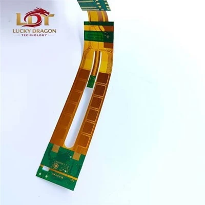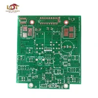

A 4 oz Heavy Copper PCB features a finished copper weight of 140 um (4 oz/sq ft) on outer and/or inner layers. Built for high-current distribution and thermal dissipation, this architecture prevents localized overheating and trace burnout. Typical stack-ups combine heavy copper planes with standard signal layers for mixed-signal power electronics.
Technical Specifications
|
Parameter |
Specification Range |
|
Finished Copper Weight |
4 oz (140 um) nominal (Outer/Inner) |
|
Layer Count |
1 to 24 layers (Hybrid heavy/signal stack-ups available) |
|
Board Thickness |
0.8 mm to 4.0 mm |
|
Min. Trace Width / Spacing |
5 mil / 5 mil (depending on copper thickness and etching parameters) |
|
Max. Board Size |
600 mm x 500 mm |
|
Surface Finishes |
ENIG, Immersion Silver, OSP, HASL (Lead-Free), Galvanic Gold (selective) |
|
Solder Mask |
High-temperature liquid photoimageable (LPI), thick-film clearance capabilities |
|
Base Materials |
FR-4 (Tg >= 170°C), Polyimide, Ceramic-filled high-frequency laminates |
Key Features
High Current Density: Accommodates continuous currents up to 50 A+ per trace depending on trace width and allowable temperature rise (30°C delta).
Thermal Management: Dissipates heat away from high-power components (MOSFETs, IGBTs) directly into internal copper planes, reducing dependence on external heat sinks.
Mechanical Strength: Withstands high mechanical vibration and thermal cycling without trace cracking or pad lifting at mounting holes.
Planar Transformer Integration: Supports embedded planar magnetics and high-frequency inductive components directly within the PCB layout.
Applications
Renewable Energy
Solar string inverters, wind turbine pitch controllers, and energy storage system (ESS) battery management units.
Electric Vehicles
On-board chargers (OBC), DC-DC converters, and motor drive inverters.
Industrial Automation
High-power variable frequency drives (VFD), servo controllers, and industrial power supplies.
Grid Infrastructure
Smart grid distribution switches and high-voltage protection relays.
Customization
Hybrid Stack-ups: Combine 4 oz power/ground planes with 1 oz or 2 oz signal layers to balance high-current capability and fine-pitch routing.
Thermal Vias: Filled and capped via-in-pad arrays under high-dissipation power packages (TO-220, D2PAK).
Controlled Depth Routing: Partial cavity milling for busbar integration or direct component seating.
Specialized Dielectrics: High-Tg (>180°C) and high-CTI (>600V) laminates for high-voltage isolation.
Quality Control
Etching Verification: Automated Optical Inspection (AOI) calibrated for thick copper edge profiles to control undercut and maintain nominal trace geometries.
X-Ray Inspection: Non-destructive testing for multi-layer inner-layer alignment and barrel crack detection in plated through-holes (PTH).
Electrical Testing: 100% flying probe or fixture test (Hi-Pot test up to 2000V DC based on insulation spacing).
In-House Testing Equipment: AOI systems, micro-section analysis labs, thermal stress testing baths, and ionic contamination testers.
Manufacturing & Certifications
Production Facility
Fully automated heavy copper etching lines, pulse plating rectifiers for uniform copper distribution, and vacuum lamination presses.
Standards Compliance
Manufactured in accordance with IPC-A-600 (Class 2/3) and IPC-6012.
Certifications
ISO 9001:2015, IATF 16949 (Automotive), ISO 13485 (Medical), and UL certified (E-file available upon request).
Packaging & Delivery
Packaging: Vacuum-sealed anti-static moisture barrier bags with desiccant and humidity indicator cards; double-walled corrugated cartons with edge protection for transit security.
Lead Time:
- Prototypes (1-4 layers): 5 to 7 working days.
- Batch Production: 12 to 18 working days depending on volume and stack-up complexity.
- Logistics: Direct air/ocean freight options via trusted international couriers (DHL, FedEx, UPS).
FAQ
Q: How do you prevent excessive copper undercut during the 4 oz etching process?
A: We utilize specialized differential etching parameters, pulse-reverse plating to optimize copper crystal grain structure, and compensation factors built into our CAM engineering step to maintain edge wall verticality within +/-15% of copper thickness.
Q: Can 4 oz copper layers be combined with fine-pitch signal layers in the same stack-up?
A: Yes. Hybrid stack-ups use 4 oz foil for dedicated power/ground planes and 1 oz or 2 oz foil for outer and inner signal layers, allowing fine-pitch routing (down to 4 mil line/space) on designated layers.
Q: What is the maximum current capacity for a 4 oz copper trace?
A: Current capacity depends on allowed temperature rise, trace width, and inner/outer layer location. According to IPC-2152 standards, a 100-mil wide outer trace in 4 oz copper typically handles roughly 15 A to 20 A for a 30°C temperature rise. Exact calculations require thermal-electrical simulation based on specific layout geometries.
Q: How do you ensure uniform copper plating inside plated through-holes (PTH)?
A: We apply DC/pulse periodic reverse (PR) electroplating combined with periodic bath agitation and chemistry monitoring. This prevents barrel thinning and ensures a minimum average copper wall thickness of 25 um inside the holes.
Q: What documentation is required to initiate an RFQ for a 4 oz heavy copper PCB?
A: Submit Gerber files (RS-274X or ODB++ format), an IPC-compliant fabrication drawing specifying finished copper weights per layer, stack-up requirements, surface finish preferences, and estimated annual usage or batch quantities.
Q: Do you perform micro-section analysis reports for heavy copper shipments?
A: Yes. Micro-section reports detailing copper plating thickness, solder mask thickness over heavy copper, and dielectric spacing are available upon request as part of our outgoing quality inspection protocol.
Request a Quote
Upload your Gerber files and fabrication specifications to receive a DFM review and formal quotation within 24 hours.
Hot Tags: 4 oz heavy copper pcb, China 4 oz heavy copper pcb manufacturers, suppliers, factory