
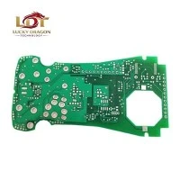
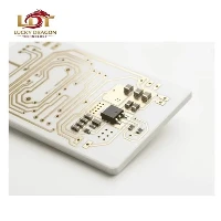

Ultra-Heavy Copper PCBs integrate copper weights from 4 oz up to 20 oz+ (and specialized designs exceeding 100 oz) within standard or hybrid stack-ups. By combining thick copper planes with standard FR4, polyimide, or high-frequency substrates, these boards route high currents, dissipate thermal loads, and form onboard heatsinks or high-current busbars directly on the circuit board.
Technical Specifications
|
Parameter |
Standard Capability |
Advanced Capability |
|
Copper Weight |
4 oz to 10 oz |
Up to 20 oz+ (Embedded busbar up to 200 oz) |
|
Layer Count |
1 to 12 layers |
Up to 24 layers (dependent on stack-up) |
|
Base Materials |
FR4 (Tg 170 C / 180 C), Nelco, Rogers |
Ceramic-filled PTFE, Polyimide |
|
Min. Trace / Space |
6 mil / 6 mil (for heavy layers) |
4 mil / 4 mil (outer layers) |
|
Max. Board Thickness |
4.0 mm |
6.5 mm |
|
Surface Finishes |
ENIG, HASL (Lead-Free), Immersion Silver, OSP |
ENEPIG, Selective Gold Plating |
|
Solder Mask |
Thick film liquid photoimageable (LPI) |
High-temperature green/black LPI |
Key Features
High Current Carrying Capacity: Handles continuous currents exceeding 100A, determined by trace width and copper cross-sectional area.
Thermal Management: Lowers junction temperatures by conducting heat away from power semiconductors (MOSFETs, IGBTs) directly to chassis or heatsinks.
Planar Transformer Integration: Enables embedded magnetic components and planar transformers within the PCB stack-up.
Mechanical Reinforcement: Provides structural rigidity for press-fit connectors and heavy screw-down terminals without cracking the board substrate.
CTE Matching: Mitigates coefficient of thermal expansion mismatches between heavy copper planes and dielectric materials during thermal cycling.
Applications
Renewable Energy
Solar string inverters, wind turbine pitch control systems, and energy storage system (ESS) power conversion units.
Electric Vehicles
On-board chargers (OBC), DC-DC converters, motor inverter drives, and high-power charging station distribution modules.
Industrial Equipment
High-power welding machines, industrial motor controllers, and heavy-duty UPS systems.
Aerospace & Defense
Radar power distribution units, actuator controls, and avionic power supplies.
Customization
Hybrid Stack-ups: Combining heavy copper inner layers (for power distribution) with fine-line outer layers (for control logic and signal routing).
Cavity & Depth Milling: Machining blind cavities or step-milling for direct component sink and thermal pad contact.
Busbar Integration: Embedding solid copper inlays or shaped copper bars directly into the PCB routing channels prior to lamination.
Thermal Via Arrays: Filled and capped thermal via arrays beneath high-dissipation power devices.
Quality Control
X-Ray Inspection: Detects internal voids in thick plated-through-holes (PTH) and evaluates copper distribution symmetry.
Microsection Analysis: Verifies copper thickness, wall plating thickness, and etch factor post-fabrication per IPC-A-600 Class 3 standards.
Automated Optical Inspection (AOI): Laser-based AOI calibrated for thick-copper etch profiles to catch undercut and bridging defects.
Electrical Testing: 100% flying probe or fixture-based testing including high-voltage isolation (Hi-Pot) and continuity checks up to 1500V.
Manufacturing & Certifications
Etching Lines: Specialized differential etching equipment utilizing step-etching chemistry to manage high aspect ratios of thick copper traces.
Plating Systems: Direct pulse-plating and DC rectification tanks engineered for uniform copper throw in deep, thick-copper plated-through holes.
Lamination Presses: Multi-daylight vacuum presses with automated thermal profiling to eliminate resin starvation in heavy copper clearance areas.
Certifications: ISO 9001:2015, IATF 16949 (Automotive), ISO 13485 (Medical), UL Listed (E-File verification available upon request), and IPC-6012 Class 3/3A compliance.
Packaging & Delivery
Packaging: Vacuum-sealed anti-static bags with active desiccant silica gel, packed in multi-layer corrugated cartons with edge protection.
Logistics: Shipped via air freight (DHL, FedEx, UPS) or sea freight with environmental data loggers for moisture-sensitive shipments.
Lead Time: Prototypes (1 to 4 layers): 7 to 10 working days. Production batches (4 to 12 layers): 15 to 25 working days based on copper weight and stack-up complexity.
FAQ
Q: How do you prevent etching undercut when producing 10 oz copper traces?
A: We use specialized acid-etch chemistry combined with multi-pass differential etching and compensated Gerber tooling. This controls the etch factor, maintaining near-vertical trace sidewalls and eliminating excessive lateral erosion.
Q: What is the maximum copper thickness you can plate inside through-holes?
A: We achieve up to 4 oz (140 um) of copper thickness inside standard plated-through holes. For higher current requirements, we utilize drilled and press-fit busbar inlays or tapped blind vias.
Q: How do you eliminate resin starvation and voids in heavy copper prepreg lamination?
A: We use high-resin-content (RC) prepregs and multi-stage vacuum lamination profiles. Flowable resin fills the deep cavities between heavy copper planes, preventing air entrapment and delamination during thermal stress.
Q: Can heavy copper layers be combined with fine-line signal layers in the same stack-up?
A: Yes. Hybrid stack-ups pair 4 oz to 20 oz power planes on inner layers with 1 oz or 0.5 oz outer layers for fine-pitch component routing (down to 4 mil line/space).
Q: What IPC standard do your heavy copper PCBs adhere to?
A: All production runs comply with IPC-A-600 Class 3 for rigid printed boards and IPC-6012 specifications, ensuring zero delamination, complete barrel fill, and strict solder mask registration.
Q: What file formats are required to generate an accurate RFQ quote?
A: Submit Gerber files (RS-274X or ODB++), an explicit layer stack-up drawing indicating copper weights per layer, drill files, and a fabrication drawing specifying surface finish, IPC class, and electrical test requirements.
Request a Quote
Upload your Gerber files, stack-up requirements, and expected annual volume to receive a DFM report and commercial quotation within 24 hours.
Hot Tags: ultra-heavy copper pcb, China ultra-heavy copper pcb manufacturers, suppliers, factory


