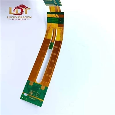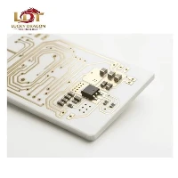
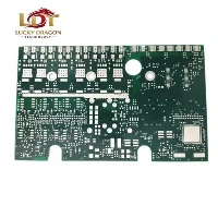

8 oz heavy copper PCBs handle high current loads and high thermal dissipation requirements that standard 1 oz to 2 oz boards cannot sustain. By depositing an 8 oz/ft^2 copper layer (nominal thickness 280 um), these boards conduct extreme currents while minimizing resistive heat generation and voltage drop. Used primarily in high-power distribution and conversion systems, they combine heavy power planes with signal circuitry on the same substrate.
Technical Specifications
|
Parameter |
Specification |
|
Base Material |
High-Tg FR4 (Tg >= 170 degree C), Polyimide, Ceramic-filled PTFE |
|
Finished Copper Weight |
8 oz (280 um) outer and/or inner layers |
|
Layer Count |
1 to 16 layers (hybrid stack-ups supported) |
|
Min. Trace Width / Spacing |
6 mil / 6 mil (dependent on copper thickness and etching parameters) |
|
Min. Finished Hole Size |
0.20 mm (mechanically drilled) |
|
Max. Board Dimensions |
600 mm x 500 mm |
|
Surface Finish |
ENIG, HASL (Lead-Free), Immersion Silver, OSP, Hard Gold |
|
Solder Mask |
High-temperature liquid photoimageable (Green, Black, Blue, Red) |
|
Board Thickness |
1.6 mm to 4.0 mm |
Key Features
High Current Capacity: Conducts high amperage per trace without excessive temperature rise or fusing.
Thermal Management: Dissipates heat away from high-power components (IGBTs, MOSFETs) directly through the copper planes to reduce thermal resistance.
Mechanical Strength: Withstands high mechanical stress, vibration, and thermal shock during cyclic loads.
Mixed-Technology Integration: Combines heavy power traces and fine-pitch control circuits on a single board layout.
Applications
Renewable Energy
Solar string inverters, wind turbine pitch controllers, and energy storage system (ESS) power management units.
Automotive Systems
Electric vehicle (EV) DC-DC converters, on-board chargers (OBC), and motor drive controllers.
Industrial Equipment
High-power welding machines, industrial power supplies, and uninterruptible power supplies (UPS).
Grid Infrastructure
Smart grid distribution switches and high-voltage relay modules.
Customization
Stack-up Engineering: Custom hybrid configurations mixing heavy copper power planes (8 oz) with standard signal layers (1 oz to 2 oz).
Plating Options: Selective heavy copper plating on specific power rails while maintaining standard copper thickness on fine-pitch areas.
Thermal Vias: Filled and capped copper-plated thermal via arrays beneath high-dissipation surface components.
Routing & Profiling: Routing tolerances down to +/- 0.10 mm, V-scoring, and edge plating for grounding or shielding.
Quality Control
Etching Inspection: Automated Optical Inspection (AOI) calibrated for heavy copper line-width compensation and undercut limits.
Inner-Layer Verification: 100% electrical testing for opens and shorts prior to lamination.
Microsection Analysis: Destructive physical analysis (DPA) to verify copper plating thickness, barrel integrity, and resin fill in plated through-holes (PTH).
Thermal Stress Testing: Solder float test at 288 degree C for 10 seconds to check for delamination and blistering.
Manufacturing & Certifications
Production Capabilities: Specialized etching lines utilizing differential pulse plating to maintain uniform copper thickness across large panels. Controlled lamination presses handle high-resin-flow prepregs required to fill deep copper gaps.
Facility Certifications:
- ISO 9001:2015 (Quality Management System)
- IATF 16949 (Automotive Quality Management)
- ISO 14001:2015 (Environmental Management)
- UL File Number: E468253 (Flame Retardant Compliance)
Packaging & Delivery
Packaging: Vacuum-sealed in anti-static moisture barrier bags with desiccant and humidity indicator cards, packed in rigid corrugated cartons with custom foam cushioning to prevent edge damage.
Lead Time:
Prototypes (1-5 pcs): 7 to 10 working days.
Batch Production: 15 to 20 working days based on volume and stack-up complexity.
Shipping: Air and ocean freight options with traceable courier tracking (DHL, FedEx, UPS) and commercial invoice documentation.
FAQ
Q: What is the minimum trace width and spacing achievable with 8 oz copper?
A: For 8 oz finished copper, the practical minimum trace width and spacing is 6 mil / 6 mil. Achieving finer geometries requires etching compensation techniques or selective copper reduction methods during layout review.
Q: How do you prevent etching undercut and ensure vertical trace sidewalls on 8 oz layers?
A: Production utilizes alkaline etching lines with automated chemical concentration and temperature controllers, combined with specialized pulse-plating parameters to maintain uniform copper distribution and minimize side-etching on thick copper features.
Q: Can 8 oz heavy copper be combined with standard 1 oz or 2 oz layers in a multi-layer stack-up?
A: Yes. Hybrid stack-ups integrate 8 oz power/ground planes with 1 oz or 2 oz signal layers. High-resin-flow prepregs are selected during lamination to completely fill voids between thick copper patterns and prevent inner-layer air pockets.
Q: What surface finishes are recommended for high-current 8 oz PCBs?
A: ENIG (Electroless Nickel Immersion Gold) or Immersion Silver are recommended. They provide flat coplanar surfaces for high-power surface-mount devices (SMDs) and prevent oxidation on exposed heavy copper pads.
Q: How is the thermal dissipation performance verified on heavy copper boards?
A: Thermal performance is validated through microsection analysis of copper thickness uniformity, combined with customer-specified thermal imaging or heat-rise testing under maximum rated operating current during prototype evaluation.
Q: What design files are required to initiate a quote and DFM review?
A: Submit standard Gerber files (RS-274X format), ODB++ files, an IPC-compliant drill file, and a complete fabrication drawing specifying copper weights, stack-up order, surface finish, and impedance control requirements.
Request a Quote
Upload your Gerber files and stack-up requirements to receive a DFM feedback report and commercial quotation within 24 hours.
[Upload Gerber Files & Get Quote]
Hot Tags: 8 oz heavy copper pcb, China 8 oz heavy copper pcb manufacturers, suppliers, factory