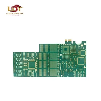

Any-Layer HDI PCB utilizes laser-drilled microvias stacked or staggered across every layer pair, bypassing traditional mechanical drilling limitations. This architecture maximizes routing density for fine-pitch BGA packages (down to 0.3mm pitch or below) in space-constrained electronic hardware. Production relies on sequential lamination cycles and direct laser ablation, ensuring reliable interlayer electrical connection without occupying internal routing channels.
Technical Specifications
|
Parameter |
Capability Specification |
|
Max Layer Count |
Up to 40 layers (Any-Layer interconnection) |
|
Min. Laser Via Size |
3 mil (75 um) / 4 mil (100 um) |
|
Min. Trace / Space (L/S) |
2.5 mil / 2.5 mil (63 um / 63 um) |
|
Board Thickness |
0.4 mm - 6.0 mm |
|
Aspect Ratio (Microvia) |
Up to 1:1 |
|
Aspect Ratio (Through-hole) |
Up to 12:1 |
|
Core Materials |
FR-4 (High Tg / Low Dk/Df, e.g., Isola, Panasonic, Shengyi), High-Frequency laminates (Rogers, Taconic) |
|
Surface Finishes |
ENIG, ENEPIG, Immersion Silver, OSP, Hard Gold |
|
Impedance Control Tolerance |
+/- 10% (Standard), +/- 5% (Strict) |
Key Features
Stack-via Capability: Microvias can be stacked directly on top of vertical interconnections across multiple sequential lamination cycles, freeing routing space on internal layers.
Controlled Dielectric Spacing: Dielectric thickness between layers is maintained within tight tolerances (+/- 10%) to preserve single-ended and differential impedance stability at multi-gigabit speeds.
Laser Direct Structuring (LDS) Compatibility: Direct copper filling of microvias prevents depression defects and ensures planar surfaces for subsequent fine-pitch component placement.
Thermal Management Integration: Supports copper filled/capped blind vias directly beneath high-dissipation IC pads to conduct thermal energy away from semiconductor junctions.
Applications
5G Telecommunications
Base station power amplifiers, high-speed transceiver modules, and backplane routing cards.
Automotive Electronics
Advanced Driver Assistance Systems (ADAS) domain controllers, LiDAR processing units, and infotainment mainboards.
High-Performance Computing (HPC)
Artificial intelligence accelerators, server motherboards, and high-density memory modules.
Medical Devices
Portable ultrasound systems, patient telemetry transmitters, and high-resolution imaging controllers.
Customization Options
Stack-up Engineering: Custom stack-up design based on signal integrity (SI) simulation, EMI shielding requirements, and mechanical thickness constraints.
Material Selection: Cross-referencing thermal expansion coefficients (CTE) against operating temperature profiles to prevent solder joint fatigue.
Surface Treatment Combinations: Selective plating options (e.g., ENIG for wire bonding areas coupled with OSP for standard SMT pads).
Mask and Legend: Liquid Photoimageable (LPI) solder mask in various colors; laser-etched permanent serial numbers or 2D barcodes for component traceability.
Quality Control & Inspection
AOI (Automated Optical Inspection): 100% inner and outer layer trace inspection using high-resolution optical sensors for short, open, and etch anomalies.
AVI (Automated Visual Inspection): Post-solder mask inspection verifying mask coverage, dam width, and pad cleanliness.
Electrical Testing: Flying probe testing for prototype/small batches; dedicated fixture bed-of-nails testing for volume production.
Reliability Testing Lab: In-house capability for microsection analysis, thermal shock testing (-65 degrees C to +125 degrees C), solder float testing, and Time-Domain Reflectometry (TDR) impedance verification.
Manufacturing & Certifications
Production Floor Infrastructure
Cleanroom environment (Class 10,000) for lamination and exposure; high-precision UV/CO2 laser drilling systems; vertical continuous plating lines for uniform copper wall thickness in microvias.
Traceability
Barcode-tracked work orders linking raw material batch numbers to final shipped panels.
Certifications
ISO 9001:2015 (Quality Management Systems)
IATF 16949 (Automotive Quality Management)
ISO 13485 (Medical Devices Quality Management)
UL Certified (E-File compliance for flammability ratings)
IPC-A-600 Acceptability of Printed Boards (Class 2 / Class 3 compliance)
Packaging & Delivery
Packaging Protocol: Vacuum-sealed anti-static bags containing desiccant packs and humidity indicator cards (HIC), cushioned with layered EPE foam inside double-wall corrugated export cartons.
Bake-Out Compliance: Moisture-sensitive level (MSL) baking protocols applied prior to vacuum sealing for boards susceptible to moisture absorption.
Logistics Partnerships: Expedited international air freight via DHL, FedEx, and UPS, or palletized sea freight for high-volume ocean consignments.
Frequently Asked Questions
Q: What is the maximum number of sequential lamination cycles your facility supports for Any-Layer HDI?
A: Production standard supports up to 3+N+3 or 4+N+4 sequential lamination cycles (totaling up to 40 layers), depending on the aspect ratio and core material selection. Engineering review of Gerber files determines the minimum layer count required for specific fan-out patterns.
Q: How do you prevent microvia reliability failure during thermal cycling (IPC-TM-650)?
A: Process control parameters focus on copper plating bath chemistry throwing power to achieve a minimum of 15 um copper thickness at the base of microvias. Additionally, conductive paste filling or copper electroplating filling with planarization prevents dimpling, eliminating stress concentration points during thermal expansion.
Q: What file formats are required for DFM analysis and quotation?
A: Submissions require ODB++ files or Gerber RS-274X data coupled with an IPC-D-356 netlist file, accompanied by a fabrication drawing specifying material type, copper weight, surface finish, and impedance control requirements.
Q: What is the standard lead time for Any-Layer HDI PCB prototyping vs. volume production?
A: Prototype lead times range from 8 to 12 working days depending on stack-up complexity and material availability. Volume production runs typically require 15 to 25 working days post-DFM sign-off and tooling approval.
Q: Can your engineering team modify existing stack-ups to meet strict differential impedance targets?
A: Yes. Pre-production engineering runs field solver simulations (using Polar Instruments software) to adjust dielectric thicknesses and trace widths, providing an optimized stack-up proposal for customer sign-off before artwork tooling release.
Q: Are all Any-Layer HDI batches tested for inner-layer connectivity before final shipment?
A: Yes. All panels undergo 100% netlist electrical testing (flying probe or fixture) matching the netlist extracted from the source ODB++ or Gerber data. Microsection coupons are evaluated for plating integrity on every production panel lot.
Request a Quote
Upload your design package to trigger an automated DFM check and direct engineering review.
Required File Inputs: ODB++ or Gerber RS-274X + IPC-D-356 Netlist, Fabrication Drawing (PDF with stack-up details), and Impedance Control Worksheet (if applicable).
Direct Engineering & RFQ Upload Portal: [Insert Secure File Upload Link / Email]
Hot Tags: any-layer hdi pcb, China any-layer hdi pcb manufacturers, suppliers, factory