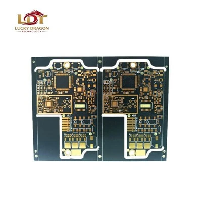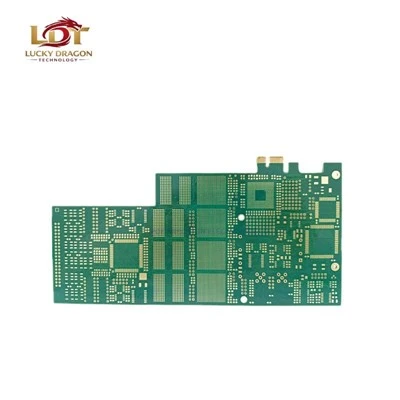


Microvia HDI PCBs utilize laser-drilled microvias (<= 150 µm diameter), fine lines, and capture pads to achieve higher circuit density per unit area than standard multilayer PCBs. Built using sequential lamination technology, these boards support fine-pitch IC packages (BGA, CSP) while optimizing routing space and reducing overall layer count. Designed for high-speed digital applications, they ensure signal integrity through controlled impedance profiles and reduced parasitic capacitance. Every project undergoes a thorough DFM (Design for Manufacturing) engineering review prior to production to optimize board layout for maximum manufacturing yield.
Technical Specifications
|
Parameter |
Specification Range |
|
Layer Count |
4 to 32+ layers |
|
HDI Structure Types |
1+N+1, 2+N+2, 3+N+3, Any-Layer HDI |
|
Minimum Trace / Space |
2.5 / 2.5 mil (63.5 / 63.5 µm) |
|
Laser Microvia Diameter |
3 mil to 6 mil (75 µm to 150 µm) |
|
Aspect Ratio (Microvia) |
Up to 1:1 |
|
Board Thickness Range |
0.4 mm to 4.5 mm |
|
Dielectric Materials |
FR-4 (High-Tg), Isola (FR408HR), Panasonic (Megtron 6/7), Rogers (RO4000 series) |
|
Surface Finishes |
ENIG, ENEPIG, Immersion Silver, OSP, HASL (Lead-Free) |
|
Impedance Tolerance |
±10% (±5% for critical nets) |
|
Manufacturing Standard |
IPC-6012 Class 2 / Class 3 / Class 3/A |
Key Features
Sequential Lamination Architecture: Enables multi-step buildup for complex blind and buried via connections without routing restrictions on internal planes.
Laser-Drilled Microvias: Replaces mechanical drilling for sub-mil apertures, creating smooth barrel walls for reliable copper plating.
Filled Via-in-Pad Technology: Plated-through microvias are filled with non-conductive or conductive epoxy and planarized, allowing direct placement of components on pads to save routing space.
Controlled Dielectric Spacers: Utilizes ultra-thin prepregs (2 mil to 3 mil) to maintain strict differential impedance and minimize electromagnetic interference (EMI).
Applications
Telecom & Networking
5G base station antenna units, optical transceivers, high-speed routers.
Automotive Electronics
ADAS LiDAR modules, infotainment processors, electronic control units (ECUs).
Datacenter & Computing
High-performance computing (HPC) motherboards, server backplanes, artificial intelligence accelerators.
Medical Devices
Portable ultrasound systems, patient telemetry monitors, digital imaging sensors.
Customization
Manufactured strictly to customer Gerber files, drill files, and fabrication drawings.
Stack-Up Optimization: Engineering review of layer configurations, material selections, and copper weight distribution (0.5 oz to 2 oz) for thermal management and signal performance.
Via Plugging & Metallization: Options include resin filling, copper filling, and via capping based on assembly and thermal dissipation requirements.
Solder Mask & Silkscreen: Multiple color options (Green, Black, Blue, White, Red) with LPI (Liquid Photoimageable) masks suited for fine-pitch component clearance.
Quality Control
Production adheres to rigorous inspection protocols to ensure batch consistency and reliability:
AOI (Automated Optical Inspection): 100% inspection of inner and outer layers for open circuits, shorts, and line width anomalies.
X-Ray Inspection: Verifies layer-to-layer registration and alignment accuracy during sequential lamination.
Flying Probe & Fixture Testing: 100% electrical continuity and isolation testing executed per netlist.
Laboratory Testing: Microsection analysis (cross-sectioning) to measure copper plating thickness in microvia barrels, thermal shock testing, and solder float testing per IPC-TM-650.
Manufacturing & Certifications
Facility Capabilities
Cleanroom environment equipped with UV/CO2 hybrid laser drilling systems, direct imaging (LDI) machines, and automatic vacuum etching lines.
System Certifications
ISO 9001:2015 (Quality Management), IATF 16949 (Automotive Quality Management), ISO 14001 (Environmental Management).
Product Compliance
UL recognized (E-number on file), RoHS compliant, and REACH compliant.
Packaging & Delivery
Packaging: Vacuum-sealed anti-static bags containing desiccant and humidity indicator cards, packed inside reinforced double-wall corrugated cartons. Moisture Barrier Bags (MBB) used for high-layer-count or hygroscopic materials.
Logistics: Express air freight (DHL, FedEx, UPS) for prototypes and volume air/ocean shipping for mass production runs. Standard delivery terms include FOB, EXW, or DDP.
Frequently Asked Questions
Q: What is the minimum laser microvia diameter and aspect ratio you can fabricate reliably?
A: Laser microvia drilling achieves a minimum diameter of 3 mil (75 µm) with a 1:1 aspect ratio, ensuring stable copper plating without internal voids.
Q: How do you control registration shift during sequential lamination cycles?
A: Registration accuracy is maintained using high-precision optical alignment tools, registration pins, and direct imaging (LDI) systems that dynamically scale artwork to compensate for material expansion or contraction during thermal press cycles.
Q: Can you handle mixed dielectric stacks combining high-speed low-loss materials with standard FR-4?
A: Yes. Hybrid stack-ups combining PTFE/low-DK materials (such as Rogers) with high-Tg FR-4 are routinely processed, provided the thermal expansion coefficients (CTE) are accounted for during engineering review.
Q: What is your standard turnaround time for HDI PCB prototypes?
A: Standard prototype lead times range from 5 to 10 working days depending on layer count, via structure complexity (e.g., 2+N+2 vs. Any-Layer), and surface finish requirements. Expedited services are available upon request.
Q: Do you perform impedance testing and provide test coupons with delivery?
A: Yes. 100% impedance testing is performed using Time Domain Reflectometry (TDR) test coupons manufactured on the same panel. An impedance test report is included with every shipment.
Q: What data formats are required to initiate an engineering review and quotation?
A: Submissions require ODB++ or Gerber RS-274X data, an IPC-compliant drill file, a fabrication drawing specifying stack-up details and material callouts, and an explicit netlist file.
Request a Quote
Submit Gerber files, stack-up requirements, and estimated volume specifications to receive a technical review, DFM feedback, and formal quotation within 24 hours.
[Upload Gerber Files & Request Quote] | [Download Capabilities PDF & Stack-up Guide]
Hot Tags: microvia hdi pcb, China microvia hdi pcb manufacturers, suppliers, factory