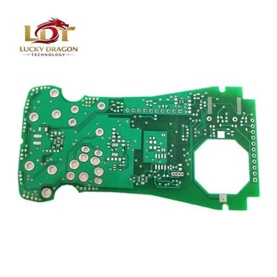

The 10-layer multilayer PCB provides high-density circuit routing for complex electronic architectures. Built with alternating signal and internal power/ground planes, this configuration separates high-speed signals from power distribution to mitigate electromagnetic interference (EMI) and maintain signal integrity. Standard stackups feature high-Tg FR-4 substrates (Tg 170°C / 180°C) paired with low-loss dielectrics to support high-frequency data transmission across industrial, telecommunications, and automotive hardware.
Technical Specifications
|
Parameter |
Standard Capability |
Advanced Capability |
|
Layer Count |
10 Layers |
10 Layers (HDI / Blind & Buried Vias) |
|
Board Thickness |
1.0mm – 3.2mm (+/-10%) |
0.6mm – 4.0mm |
|
Base Material |
FR-4 (Tg 130°C, 150°C, 170°C), Isola, Rogers |
High-Frequency / High-Speed Laminates |
|
Copper Weight |
Outer: 1 oz / 2 oz; Inner: 0.5 oz / 1 oz |
Outer up to 3 oz; Inner up to 2 oz |
|
Min. Trace Width / Spacing |
3.5 mil / 3.5 mil (0.09mm) |
3.0 mil / 3.0 mil |
|
Min. Mechanical Drill Size |
0.20 mm |
0.15 mm |
|
Min. Laser Drill Size |
N/A (Standard Through-Hole) |
0.10 mm (4 mil) |
|
Surface Finish |
HASL, ENIG, Immersion Silver, OSP, ENEPIG |
ENIG + Hard Gold Fingers |
|
Impedance Tolerance |
+/-10% |
+/-5% |
|
Max. Board Dimensions |
500 mm x 600 mm |
600 mm x 1200 mm |
Key Features
Controlled Impedance Routing: Multi-layer reference planes maintain stable characteristic impedance (+/-5% or +/-10%) for differential pairs.
Optimized Power Distribution: Dedicated inner planes for VCC and GND reduce voltage drop and power rail noise in high-frequency circuits.
Thermal Management: Thick copper options (up to 2 oz inner layers) dissipate high thermal loads generated by power MOSFETs and microprocessors.
Strict Registration Control: Automated optical alignment limits layer-to-layer displacement during lamination to prevent open/short defects in fine-pitch BGA areas.
Applications
Telecommunications
5G base station sub-assemblies, core routers, optical network terminals.
Industrial Automation
PLC mainboards, high-speed motion controllers, robotic drive units.
Medical Devices
Ultrasound signal processing units, patient monitor mainboards, diagnostic imaging hardware.
Automotive Electronics
Advanced Driver Assistance Systems (ADAS) processing units, telematics control units.
Customization Options
Stackup Engineering: Custom dielectric thickness matching specific transmission line requirements, co-designed with customer Gerber data alongside complimentary DFM (Design for Manufacturing) review prior to production tooling.
Material Selection: Integration of high-frequency laminates (e.g., Rogers RO4000 series) for RF sections combined with standard FR-4 for digital control sections (Hybrid PCB).
Solder Mask & Silkscreen: Standard green, black, blue, red, white, or yellow liquid photoimageable solder mask; customized legend markings.
Edge Processing: Castellated holes, V-cut scoring, edge plating, and router milling to specific dimensional tolerances.
Quality Control
AOI (Automated Optical Inspection): 100% inner layer and outer layer trace inspection prior to lamination and etching.
Flying Probe & Fixture Testing: 100% electrical continuity and isolation testing executed on every production panel.
Impedance Verification: TDR (Time Domain Reflectometry) testing performed on test coupons included in each manufacturing panel.
Microsection Analysis: Destructive physical analysis evaluating copper thickness, via wall plating thickness, and dielectric spacing per cross-section batch.
Manufacturing & Certifications
Production Infrastructure
Fully automated LDI (Laser Direct Imaging) exposure lines, vacuum lamination presses, and CNC drilling centers.
Process Control
Statistical Process Control (SPC) monitored across electroplating and etching lines to maintain consistent via wall thickness (> 20 um).
Factory Certifications
ISO 9001:2015 Quality Management System
IATF 16949 Automotive Quality Management
ISO 13485 Medical Devices Quality System
Compliance Standards
IPC-A-600 (Class 2 / Class 3), UL Certified (E-file available upon request), RoHS and REACH compliant.
Packaging & Delivery
Volume Scalability: Supports scalable manufacturing transitions from low-volume prototype builds directly to medium-volume batch production without tooling reconfiguration.
Packaging Configuration: Vacuum-sealed anti-static bags containing desiccant, interspersed with shock-absorbing foam layers inside reinforced double-wall corrugated cartons.
Traceability: Barcode labeling on packaging indicating batch number, layer count, date code, and panel count.
Shipping Methods: Express air freight for prototypes (DHL, FedEx, UPS) and palletized ocean/air freight for mass production batches.
FAQ
Q: What is the standard lead time for 10-layer PCB prototypes?
A: Standard prototype production takes 5 to 7 working days. Expedited 3-day service is available for urgent design validations.
Q: Do you provide impedance simulation and DFM checks before production?
A: Yes. Engineering teams execute free DFM checks and review stackup parameters, providing calculated trace widths/spacings for specified target impedances prior to tooling production.
Q: What file formats are required for quotation and production?
A: Gerber RS-274X data, ODB++ format, along with an explicit drill file and a fabrication drawing specifying stackup, material requirements, and surface finish.
Q: Can you manufacture 10-layer PCBs with blind and buried vias?
A: Yes. Sequential lamination processes support HDI 10-layer constructions utilizing microvias (e.g., 1-8-1 or 2-6-2 structures).
Request a Quote
Upload Gerber files or fabrication specifications to receive a formal quotation within 24 hours.
Required Input Data: Gerber files, layer count, board dimensions, quantity, material type, surface finish, and target delivery date.
Direct Inquiry: [Link to RFQ Form / Email Contact]
Hot Tags: 10-layer multilayer pcb, China 10-layer multilayer pcb manufacturers, suppliers, factory