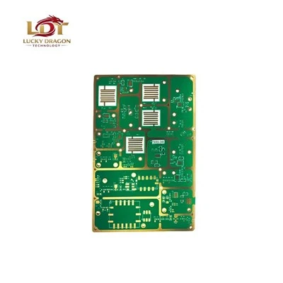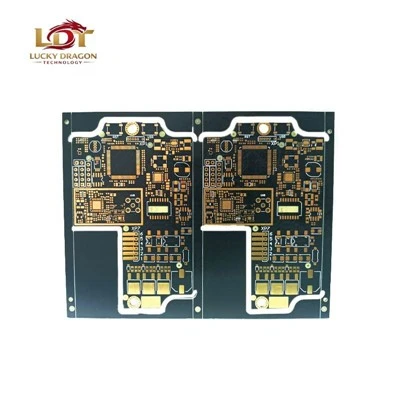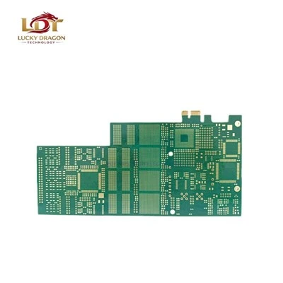
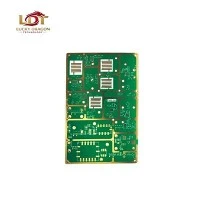

High-Density Interconnect (HDI) PCBs provide higher wiring density per unit area than standard printed circuit boards. Utilizing laser-drilled microvias (typically <= 6 mil), sequential lamination, and fine-line etching, HDI technology reduces overall board size and weight while improving electrical performance through shorter signal paths. Configured from standard 1+N+1 up to Any-Layer structures for complex digital and RF routing.
Technical Specifications
|
Parameter |
Standard Capability |
Advanced Capability |
|
Layer Count |
Up to 16 Layers |
Up to 32+ Layers (Any-Layer) |
|
Min. Trace / Space |
3 / 3 mil (75 / 75 um) |
2 / 2 mil (50 / 50 um) |
|
Min. Laser Microvia |
4 mil (100 um) |
3 mil (75 um) |
|
Aspect Ratio (Microvia) |
1:1 |
Up to 0.8:1 |
|
Board Thickness |
0.4 mm - 3.2 mm |
0.2 mm (Ultra-thin core options) |
|
Dielectric Materials |
FR-4 (Tg 170 deg C, 180 deg C), Polyimide |
Megtron 6, Rogers RO4000 series, Isola |
|
Surface Finish |
ENIG, Immersion Silver, OSP, HASL |
Electrolytic Gold, Hard Gold (Edge connectors) |
|
Impedance Tolerance |
+/- 10% |
+/- 5% (Controlled via TDR testing) |
Key Features
Sequential Lamination: Supports multiple lamination cycles for complex blind and buried via stacking (e.g., 2+n+2 structures).
Laser Microvia Formation: CO2 and UV laser drilling enables precise ablation through specific dielectric layers without damaging underlying copper pads.
Fine-Line Etching: Subtractive and modified semi-additive processes (mSAP) achieve precise impedance control and high-density pin-grid array (PGA) escape routing.
Via-in-Pad Technology: Plated-over microvias placed directly on component pads eliminate fan-out routing space and minimize parasitic inductance.
Applications
Telecommunications
5G base station antenna modules, high-speed optical transceivers, and routers.
Medical Devices
Portable ultrasound equipment, patient monitors, and implantable diagnostic tools.
Industrial & Automotive
Advanced driver-assistance systems (ADAS) processors, industrial IoT gateways, and motor controllers.
Aerospace & Defense
Avionics navigation systems and satellite communication payloads.
Customization
Stackup Engineering: Custom impedance modeling using Polar Si8000 based on specific dielectric constants (Dk) and core thicknesses.
Material Selection: Tg-rated FR-4, low-loss high-frequency laminates, or thermal management substrates (Aluminum/Copper bases integrated into HDI stackups).
Via Treatment: Copper-filled and capped microvias (via-in-pad planarized by electroplating and resin plugging) for BGA density reduction.
Solder Mask & Silkscreen: LPI solder mask in green, black, blue, or white; high-resolution white/yellow legends.
Quality Control
AOI & AOI/AXI: Automated Optical Inspection on inner/outer layers alongside Automated X-ray Inspection for hidden inner-layer registration and multi-layer alignment.
Electrical Testing: Flying probe testing for prototypes; dedicated fixture-based dual-sided grid testing for volume production (shorts/opens isolation tested at 250V to 500V).
Metallographic Microsectioning: Destructive physical analysis per IPC-TM-650 to verify copper wrap thickness, microvia barrel plating integrity, and solder mask thickness.
Reliability Screening: Thermal stress testing (288 deg C solder float), peel strength testing, and ionic contamination analysis.
Manufacturing & Certifications
Production Floor: Equipped with Hitachi high-speed CNC drilling/routing machines, Schmoll UV/CO2 laser drills, Orbotech direct imaging (LDI) systems, and automatic horizontal copper plating lines.
Process Control: Statistical Process Control (SPC) monitored across lamination press cycles and etch chambers to maintain dimension stability within +/- 0.05%.
Compliance & Standards: ISO 9001, IATF 16949, ISO 14001, UL recognized (E-number matching IPC Class 2 and Class 3 requirements). IPC-A-600 Class 2/3 execution.
Packaging & Delivery
Packaging: Vacuum-sealed anti-static moisture-barrier bags with silica gel packs and humidity indicator cards (HIC), cushioned in rigid double-wall corrugated cartons.
Logistics: Shipped via air freight (DHL, FedEx, UPS) or sea freight with commercial invoices, certificate of conformance (CoC), and microsection test reports included.
Lead Times: Prototype builds (2 to 10 layers): 5 to 8 business days; Volume production: 12 to 20 business days subject to stackup complexity.
FAQ
Q: What is the minimum blind via size your laser drills support?
A: Standard production supports a finished microvia hole size of 4 mil (100 um) with a capture pad requirement of at least 10 mil (250 um).
Q: Can you handle stackups involving mixed dielectric materials (hybrid stackups)?
A: Yes. We regularly process hybrid constructions combining high-speed low-loss materials (e.g., Rogers) with standard FR-4 outer layers to balance signal integrity and fabrication cost.
Q: How do you prevent microvoiding in stacked microvias?
A: Stacked vias undergo optimized pulse-plating copper filling parameters followed by chemical-mechanical planarization (or resin filling plus electroplated cap plating) to ensure void-free copper continuity before subsequent lamination.
Q: What impedance test documentation is provided with delivery?
A: Every production panel with controlled impedance requirements includes a TDR (Time Domain Reflectometry) test coupon report verifying trace impedances within the specified +/- 10% (or +/- 5%) tolerance band.
Q: Do you perform DFM checks prior to manufacturing?
A: Yes. Engineering teams review all incoming Gerber, ODB++, and drill files for etching tolerances, acid traps, aspect ratio limits, and thermal relief issues before tooling release.
Q: Are your HDI boards compliant with IPC Class 3 standards?
A: Manufacturing capabilities meet both IPC-A-600 Class 2 and Class 3 specifications, with Class 3 inspection criteria applied to aerospace and medical projects upon specification.
Request a Quote
Submit your Gerber or ODB++ fabrication files, layer stackup drawing, and quantity requirements directly through our secure engineering portal or email to receive a complete DFM evaluation and commercial proposal within 24 hours.
Hot Tags: high-density interconnect pcb, China high-density interconnect pcb manufacturers, suppliers, factory