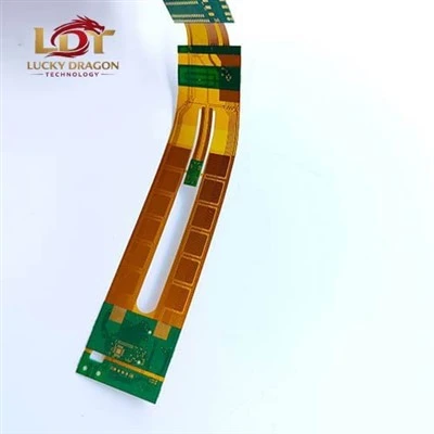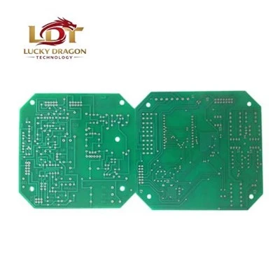

6 oz heavy copper PCBs feature a copper weight of 210 grams per square meter (approximately 210 um or 8.3 mils) per layer. This architecture handles high current loads exceeding 50A and manages severe thermal dissipation directly on the board level. Built for high-power electronics, these boards integrate control circuitry and high-current power distribution onto a single platform, eliminating external busbars and heavy wiring harnesses.
Technical Specifications
|
Parameter |
Standard Capability |
Advanced Capability |
|
Copper Weight |
6 oz (Finished) |
Up to 10 oz (Outer/Inner) |
|
Layer Count |
1 to 16 Layers |
Up to 24 Layers |
|
Base Material |
FR4 (Tg 170°C, 180°C) |
Isola, Rogers, Aluminum-backed |
|
Min. Trace / Space |
6 mil / 6 mil (for 6 oz) |
5 mil / 5 mil (subject to engineering review) |
|
Finished Board Thickness |
1.6 mm - 3.2 mm |
Up to 6.0 mm |
|
Min. Finished Hole Size |
0.3 mm |
0.25 mm |
|
Surface Finish |
ENIG, HASL (Lead-free), OSP |
Immersion Silver, ENEPIG |
|
Max. Board Size |
500 mm x 600 mm |
600 mm x 1200 mm |
|
Solder Mask |
Green, Black, Blue (High-temp) |
Double-print for thick copper edges |
Key Features
High Current Density: Conducts continuous high currents up to 100A+ depending on trace width and temperature rise limits, calculated per IPC-2152 standards.
Thermal Management: Lowers thermal resistance by using thick internal and external planes to sink heat away from high-power MOSFETs and IGBTs.
Mechanical Robustness: Withstands severe vibration and mechanical shock in industrial and automotive environments.
Direct Busbar Integration: Combines power and control layers, reducing overall assembly weight and interconnect resistance.
Applications
Renewable Energy
Solar string inverters, wind turbine pitch control units, and energy storage systems (ESS).
Electric Vehicles
DC-DC converters, on-board chargers (OBC), and motor drive controllers.
Industrial Equipment
High-power welding machines, industrial motor drives, and uninterruptible power supplies (UPS).
Telecommunications
High-power RF amplifiers and base station power distribution units.
Customization
Manufactured strictly to Gerber files and fabrication drawings.
Mixed Copper Weights
Combine standard signal layers (1 oz or 2 oz) with 6 oz power planes within the same multilayer stackup.
Thermal Vias
Filled and capped via arrays (VIPPO) directly under high-dissipation components using non-conductive or conductive epoxy.
Contour Routing
Step V-cuts, deep milling, and edge plating for chassis grounding and shielding.
Quality Control
X-Ray Inspection: Verifies barrel-to-pad alignment and detects inner-layer voids in heavy copper plating.
Automated Optical Inspection (AOI): Detects etching anomalies, shorts, and line width reductions on thick copper layers.
Flying Probe & Bed of Nails Testing: 100% electrical continuity and isolation testing at 250V-500V test voltages.
Microsection Analysis: Destructive physical analysis performed per lot to verify copper thickness, plating distribution in plated-through-holes (PTH), and solder mask encapsulation.
Manufacturing & Certifications
Production Equipment: Direct Imaging (DI) exposure systems for accurate trace registration over thick copper profiles; specialized high-frequency etching lines configured for deep copper removal.
Facility Standards & Compliance: ISO 9001:2015, IATF 16949 (Automotive), ISO 13485 (Medical), UL 94V-0 flammability certification, and ITAR/DFARS compliance available upon request for defense and aerospace projects.
IPC Compliance: Built and inspected to IPC-A-600 Class 2 or Class 3, and IPC-6012.
Packaging & Delivery
Packaging: Vacuum-sealed in moisture-barrier bags with desiccant and humidity indicator cards; cushioned with high-density EPE foam inside double-wall corrugated cartons to prevent edge chipping during transit.
Lead Time Transparency: Prototypes (5 to 8 layers with 6 oz): 7 to 10 working days; Production batches: 15 to 20 working days following engineering query (EQ) sign-off.
Frequently Asked Questions
Q: How do you prevent etching undercut when processing 6 oz copper layers?
A: We use differential etching parameters combined with compensation factors in our CAM software, paired with pulse-plating techniques to ensure vertical trace sidewalls and minimal undercut on 210 um thick copper.
Q: Can 6 oz copper layers be combined with standard 1 oz signal layers in a multilayer stackup?
A: Yes. Asymmetric hybrid stackups integrating 6 oz power/ground planes and 1 oz signal layers are standard practice. Engineering review of the stackup is required to control bow and twist during lamination.
Q: What is the minimum clearance required between 6 oz copper traces to avoid bridging?
A: For 6 oz finished copper, we recommend a minimum trace-to-trace spacing of 8 mils (0.2 mm) to ensure reliable solder mask dam formation and prevent electrical shorts during etching and reflow.
Q: How do you ensure complete solder mask coverage over heavy copper trace steps?
A: We apply specialized high-viscosity liquid photoimageable (LPI) solder masks using double-pass coating methods, or employ resin plug-and-cap processes to level thick copper features prior to mask application.
Q: What is your standard compliance level for heavy copper PCBs?
A: All production runs comply with IPC-6012 specifications. We manufacture to IPC-A-600 Class 2 for industrial use or Class 3 for high-reliability automotive and aerospace applications upon request, backed by UL-certified laminate materials.
Q: What file formats are required for quotation and manufacturing?
A: Standard Gerber RS-274X or ODB++ files, accompanied by an IPC-compliant fabrication drawing specifying finished copper weights, stackup details, and surface finish requirements.
Request a Quote
Upload your Gerber files, stackup requirements, and estimated annual volume to receive a DFM (Design for Manufacturing) review and quotation within 24 hours.
[Upload Gerber Files & Request Quote]
Hot Tags: 6 oz heavy copper pcb, China 6 oz heavy copper pcb manufacturers, suppliers, factory