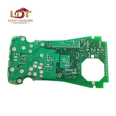

The 12-Layer Multilayer PCB routes dense netlists across multiple signal, power, and ground planes. Dedicated internal ground and power planes isolate sensitive analog signals from high-speed digital switching noise, reducing electromagnetic interference (EMI). Fabricated using sequential lamination and laser microvias where required, this board structure supports complex routing in space-constrained enclosures.
Technical Specifications
|
Parameter |
Standard Capability |
Advanced Capability |
|
Layer Count |
12 Layers |
Up to 16+ Layers |
|
Board Thickness |
1.60 mm |
0.80 mm to 3.20 mm |
|
Min. Trace / Space |
3.5 mil / 3.5 mil (0.09 mm) |
3.0 mil / 3.0 mil |
|
Min. Drill Hole Size |
0.20 mm (Mechanical) / 0.10 mm (Laser) |
0.15 mm / 0.075 mm |
|
Copper Weight |
Outer: 1 oz (35 um) / Inner: 0.5 oz to 1 oz |
Outer: up to 3 oz / Inner: up to 2 oz |
|
Material Types |
FR-4 (Tg 130C, 150C, 170C) |
High-Tg FR-4, Megtron 6, Rogers RO4000 series |
|
Surface Finish |
ENIG, HASL Lead-Free, Immersion Silver |
OSP, Hard Gold, Immersion Tin |
|
Solder Mask Color |
Green, Black, Blue, Red, White, Matte options |
Custom color matching |
|
Impedance Tolerance |
+/- 10% |
+/- 5% |
|
Max Board Size |
500 mm x 600 mm |
600 mm x 1200 mm |
Key Features
Controlled Impedance Stackup: Symmetrical layer construction prevents board warpage and maintains strict +/- 5% to +/- 10% single-ended and differential impedance control for high-speed signal integrity.
Internal Plane Distribution: Dedicated internal split planes isolate power rails, suppress voltage ripple, and provide low-inductance return paths.
High Aspect Ratio Plating: Plating through-holes with an aspect ratio up to 10:1 ensures reliable barrel copper thickness and prevents micro-cracks during thermal cycling.
Via-in-Pad Capability: Filled and plated over vias (VIPPO) allow high-density BGA fanout, reducing routing inductance and saving real estate.
Applications
Telecommunications
5G base station remote radio units, core network switches, and optical transceivers requiring high-frequency signal retention.
Medical Devices
Ultrasound imaging systems, patient monitoring consoles, and MRI data acquisition units requiring strict compliance with reliability standards.
Industrial Automation
Multi-axis motion controllers, high-speed PLC backplanes, and robotic drive units operating in harsh vibration environments.
Automotive Electronics
Advanced Driver Assistance Systems (ADAS) processing units, LiDAR interface boards, and electric vehicle powertrain controllers.
Customization
Stackup Design: Custom dielectric thickness assignment based on customer-provided impedance calculation reports (Polar SI9000).
Material Selection: Integration of low-loss laminate materials for high-frequency RF transmission or high-temperature resin systems for thermal endurance.
Blind and Buried Vias: Support for staggered, stacked, or sequential blind/buried via architectures to resolve complex routing congestion.
Edge Plating & Castellated Holes: Board edge metallization for chassis grounding/EMI shielding, and castellated holes for module-to-module daughterboard mounting.
Quality Control
AOI (Automated Optical Inspection): 100% inspection of inner and outer layers post-etching to detect short circuits, opens, and line width anomalies.
Flying Probe & Fixture Testing: 100% electrical continuity and isolation testing executed on all finished lots based on netlist data (IPC-CC-830 standards).
X-Ray Inspection: Layer-to-layer registration verification to check for core shift and ensure annular ring integrity.
Microsection Analysis: Destructive physical analysis performed per production lot to measure copper plating thickness, dielectric spacing, and hole wall integrity.
Thermal Stress Testing: Sample coupons subjected to solder float testing at 288C for 10 seconds to screen for delamination or barrel cracking.
Manufacturing & Certifications
Fabrication Facility
Fully equipped cleanroom environment utilizing direct imaging (DI) exposure systems, high-speed CNC drilling routers, and vacuum lamination presses.
Process Control
Statistical Process Control (SPC) monitored across chemical etching, electroplating, and solder mask curing stages.
Certifications
ISO 9001:2015 Quality Management System
IATF 16949 Automotive Quality Management
ISO 13485 Medical Devices Quality Management
UL Certified (E-File verification available upon request)
RoHS and REACH Environmental Compliance
Packaging & Delivery
Packaging: Vacuum-sealed anti-static bags loaded with desiccant and humidity indicator cards, cushioned with heavy-duty corrugated cartons to prevent edge impact and moisture absorption during transit.
Shipping Methods: Express air freight (DHL, FedEx, UPS) for time-critical prototypes; sea or consolidated air freight for volume production runs.
Lead Time:
- Prototype (1 to 5 layer sets): 5 to 7 business days.
- Standard Volume Production: 10 to 15 business days.
- Expedited service available upon engineering review.
FAQ
Q: What file formats are required to initiate a 12-layer PCB fabrication order?
A: Gerber RS-274X or ODB++ manufacturing files, accompanied by an IPC-compliant drill file and a fabrication drawing specifying board thickness, surface finish, and stackup requirements.
Q: How do you handle impedance control verification for high-speed layers?
A: Coupons are integrated onto the production panel matching the customer's trace width and spacing parameters. These test coupons are destructively and non-destructively tested using TDR (Time Domain Reflectometry) equipment prior to shipment.
Q: What is your standard drill-to-copper clearance for inner layers?
A: A minimum clearance of 8 mil (0.20 mm) from drill edge to internal copper plane is maintained to prevent electrical shorts during mechanical drilling and expansion.
Q: Can you process blind and buried vias in a 12-layer sequential stackup?
A: Yes. We support up to three lamination cycles, accommodating complex sequential blind and buried via structures such as 1-2, 2-11, and 11-12 configurations.
Q: What is the maximum panel utilization size for production optimization?
A: Our standard fabrication panel size is 18 x 24 inches (457 x 610 mm), with an optimal working area of 16 x 22 inches to ensure edge clamping stability during wet processing.
Q: Do you provide an official Certificate of Compliance (CoC) with every shipment?
A: Yes. Every delivery includes an inspection report and a CoC detailing material lot numbers, IPC class compliance, and electrical test verification results.
Request a Quote
Submit your Gerber files, stackup specifications, and quantity requirements to receive a formal DFM (Design for Manufacturing) review and cost estimate within 24 hours.
[ Upload Gerber Files & Request Quote ]
Hot Tags: 12-layer multilayer pcb, China 12-layer multilayer pcb manufacturers, suppliers, factory